Bob Baddeley writes on Hackaday:
PCB Design Guidelines to Minimize RF Transmissions
There are certain design guidelines for PCBs that don’t make a lot of sense, and practices that seem excessive and unnecessary. Often these are motivated by the black magic that is RF transmission. This is either an unfortunate and unintended consequence of electronic circuits, or a magical and useful feature of them, and a lot of design time goes into reducing or removing these effects or tuning them.
You’re wondering how important this is for your projects and whether you should worry about unintentional radiated emissions [..]
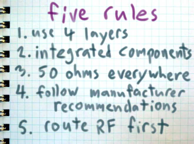
Another good guide is Michael Ossmann’s simple RF design rules: