Sven Gregori on Hackaday.io created a KiCad component and footprint for the Nokia 5110 LCD and created this breakout board to test it: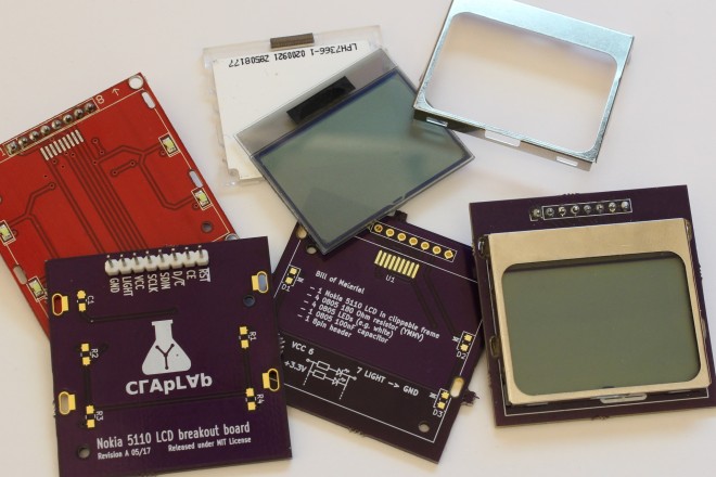
Yet another Nokia 5110 LCD breakout board
I just shamelessly measured all there was to measure and created my own KiCad PCB footprint, along with a schematic component.
Once done, I needed a way to verify it would actually work and fit the LCD, so despite how pointless it is, I created my own breakout board as proof of concept and ordered it from OSH Park.
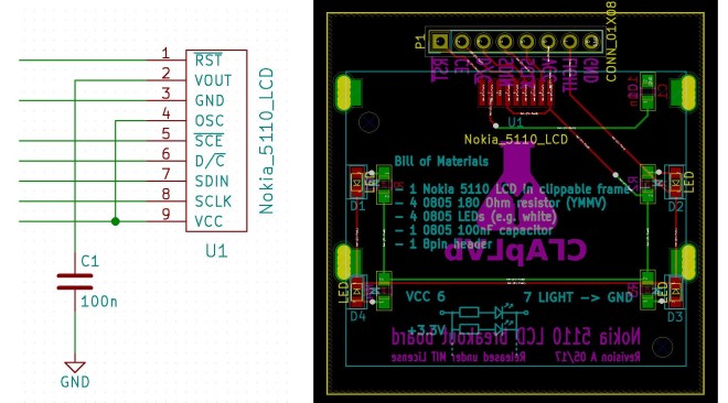
The Nokia 5110/3310 LCD and footprint are available on GitHub:


sgreg has shared the breakout board on OSH Park:
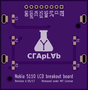
Nokia 5110 LCD Breakout Board Rev.A
![]()

Great work. I can make a circuit symbol and component footprint in KiCAD and I can make a 3D model in Wings3D. But how can I make them all into a 3D component for KiCAD? Any help would be much appreciated.
Thanks.
LikeLiked by 1 person
I’d recommend sending Sven a message on hackaday.io https://hackaday.io/sgreg
LikeLike
I can also make 3D models with DesignSpark Mechanical. See my YT videos: https://youtu.be/MdQB96fkAAk
and
LikeLiked by 1 person
very nice!
LikeLiked by 1 person
Forgot to mention – thanks for the info – I will contact Sven on hackaday.
LikeLiked by 1 person