From the FOSSi Foundation blog:
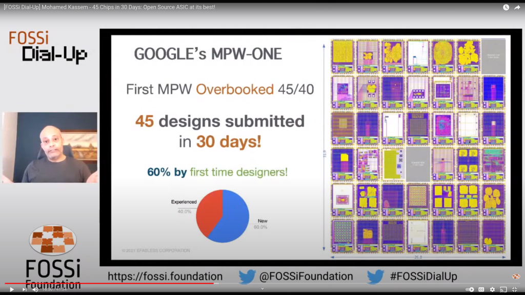
45 Chips in 30 Days: Open Source ASIC at its best!
Only seven months ago, open source chips were a dream of some, and clearly impossible to others. Today we know better. In a joint effort between efabless, Google, and the SkyWater foundry, everybody got a chance to send an open source chip to fabrication. And many did!
One of the key people who made all of that happen is Mohamed Kassem, co-founder and CEO of efabless. He joined us at FOSSi Dial-Up to discuss how the “Open MPW” program went so far. (A recording of the talk is available on YouTube.)
Efabless wants to enable everyone to produce chips. As previous talks in the FOSSi Dial-Up series have shown, getting to this point requires solving a huge amount of technical, legal, and financial challenges. Taken together they made it unthinkable for hobbyists, many in academia, and even for small companies to produce their own chips. Thankfully these initial hurdles are of the past. Once the innovative power of the open source community was unleashed, many of the projects associated with the Open MPW shuttle saw an exponential rise in interest.
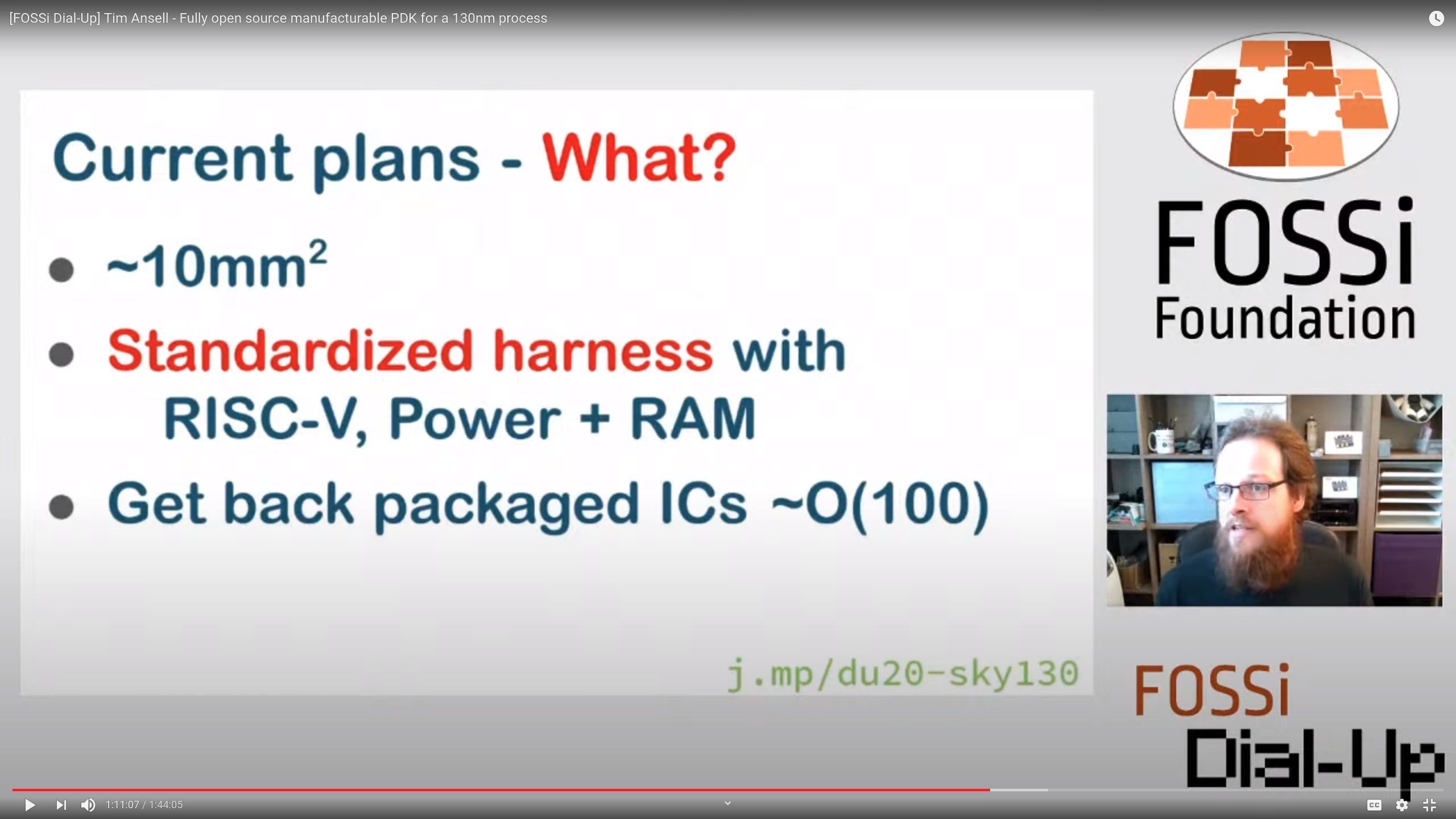
With interest exploding there was a lot to learn for everybody involved. Efabless, Google, and SkyWater prepared for that even before the Open MPW program was announced by producing three test chips, which were intended to validate the tooling and especially the SRAM components of the chip. An experience that paid off when they put together the Caravel Harness SoC, a “frame” with a 10mm² space in the middle for the actual chip design.