Introducing EDeA: An Open Platform for Easily Reusable Subcircuits

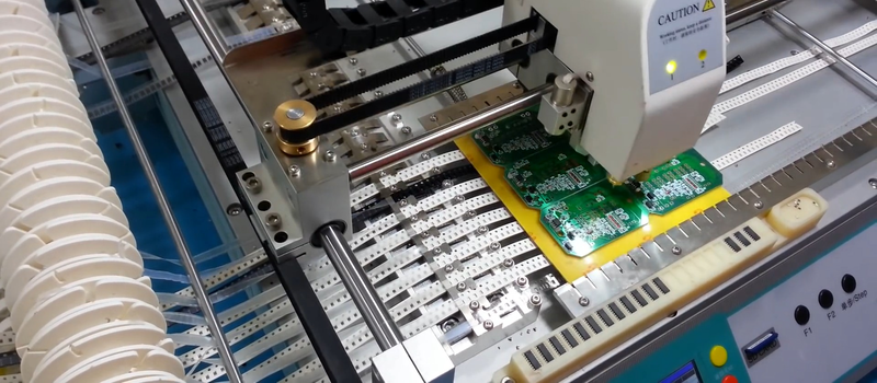
This looks like a promising way to make PCB design more efficient by leveraging the existing open source hardware designs:

Screenshot from 2020-07-30 11-02-22

Introducing EDeA

We’re building an open-source web portal for sharing KiCad subcircuits, which will enable you to create more by doing less.

This is what inspired the EDeA project. Out of a very naïve “how hard can this be?” question, we first built a primitive prototype tool to merge KiCad projects, including their schematics and PCB layout. This still need a lot of work before it can be considered safe, including correct net aliasing, nesting of subschematics, etc. But this solves only one part of the problem, something which should be solved in the upcoming major release of KiCad anyways.

We are now laying the groundwork for EDeA; a community portal to share, find, and assemble subcircuits into KiCad projects. It’s all in rough shape, and we’re still a bit away from the first alpha we will show to the public, but we’re getting there.

What we envisioned is an easy-to-use catalog of various circuit submodules; power supplies, data converters, microcontrollers, processors, and so on. These submodules contain schematics and a PCB layout, among with useful metadata; number of copper layers, component count, surface area, necessary manufacturing capabilities, and so on. Each of the subcircuit category should also have meaningful parameters; for example efficiency for a power supply, bandwidth for a transceiver. You can select any amount of these submodules, click a button, and get a KiCad project which contains all the submodules as hierarchical subsheets. Now you only need to wire these together as you need them, and in pcbnew move the already layouted submodules to fit the exact shape you need. To keep the already complex project manageable, we can’t go into auto-connecting and auto-placing of submodules. At least not yet.

Introducing EDeA: An Open Platform for Easily Reusable Subcircuits

Cool Tools: Deus Ex Autorouter

The first thing you probably asked yourself when learning how to lay out PCBs was “can’t the computer do this?” which inevitably led to the phrase “never trust the autorouter!”. Even if it hooks up a few traces the result will probably be strange to human eyes; not a design you’d want to use.

But what if the autorouter was better? What if it was so far removed from the autorouter you know that it was something else? That’s the technology that JITX provides. JITX is a company that has developed new tools that can translate a coarse textual specification of a board to KiCAD outputs autonomously.

How do you use JITX? At this point the company provides a front end to their tools; you use their website contact form to talk to a human (we assume) about what you want to make and how. But watching their demo videos (see the bottom of this post) gives a hint about how the tooling actually works. In brief; it takes a specification in a domain specific language that describes the components to use, then compiles (synthesizes?) that into KiCAD files that can be sent to fab.

via Cool Tools: Deus Ex Autorouter — Hackaday

Quote

Creating KiCad Parts From A PDF Automagically


For anyone out there who has ever struggled finding a part for Eagle or KiCad, there are some who would say you’re doing it wrong. You’re supposed to make your own parts if you can’t find them in the libraries you already have. This is really the only way; PCB design tools are tools, and so the story goes you’ll never be a master unless you can make your own parts.

That said, making schematic parts and footprints is a pain, and if there’s a tool to automate the process, we’d be happy to use it. That’s exactly what uConfig does. It automatically extracts pinout information from a PDF datasheet and turns it into a schematic symbol.

via Creating KiCad Parts From A PDF Automagically — Hackaday

Quote

Retro CPC Dongle: advise on tented vias

Advice from the Intelligent Toasters blog on how to do tented vias in DesignSpark PCB software:

Retro CPC Dongle – Part 37

Tented Vias – who’d have thought they play such an essential role? If you have no idea what tented vias are, then you’re not alone and I’m here to enlighten you.


Quote

Kicad: Designing With Complex Shapes

Screenshot from 2018-07-10 11-57-36.png

KiCad presentation by Andrew Sowa at Teardown 2018:

Kicad: Designing With Complex Shapes

While most PCBs can be simple rectangles, sometimes the design requires more complex geometry. EDA tools don’t always make this simple, so we will go over a few KiCad tips to make it easier. In this talk you will learn how to import unique board shapes from Fusion 360, create arbitrary fill zones using images, and embed high-frequency RF filters. We will use multiple software packages to enhance KiCad’s performance beyond its obvious use.

Kicad: Designing With Complex Shapes

Friday Hack Chat: Trusting The Autorouter

For this week’s Hack Chat, we’re talking about trusting the autorouter. The autorouter is just a tool, and like any tool, it will do exactly what you tell it. The problem, therefore, is being smart enough to use the autorouter.

Our guest for this week’s Hack Chat is Ben Jordan, Director of Community Tools and Content at Altium. Ben is a Computer Systems engineer, with 25 years experience in board-level hardware and embedded systems design. He picked up a soldering iron at 8, and wrote some assembly at 12. He’s also an expert at using an autorouter successfully.

via Friday Hack Chat: Trusting The Autorouter — Hackaday

Friday Hack Chat: Trusting The Autorouter

State of KiCad this Friday

kicadhackchat-01.png
Wayne Stambaugh from the KiCad project be joining Hack Chat on Hackaday.io this Friday to discuss upcoming plans and features for 2018:

kicad2

The State of KiCad

Friday, January 5, 2018 12:00 pm PST

  • What new features are on the roadmap for 2018?
  • What new features were developed since we chatted in January 2017?
  • Under the hood- how KiCad development works
  • How can a developer get started helping out?

Screenshot from 2018-01-02 23-27-04.png

State of KiCad this Friday

Designing PCBs for Assembly

Designing pcbs for assembly is easy, right? We just squirt all the footprints onto a board layout, connect all the traces, send out the gerbers and position files, and we’re done–right? Whoa, hold the phone, there, young rogue! Just like we can hack together some working source code with variables named after our best friends, we can also…

via Designing for Fab: a Heads-Up before Designing PCBs for Professional Assembly — Hackaday

Designing PCBs for Assembly

KiCAD Best Practices: Library Management

One common complaint we hear from most new KiCAD users relates to schematic and footprint libraries. The trick is to use just one schematic symbol and footprint library each with your project. This way any changes to the default schematic libraries will not affect your project and it will be easy to share your project with others without breaking…

via KiCAD Best Practices: Library Management — Hackaday

eeschema_lib.png

KiCAD Best Practices: Library Management

KiCad at FOSDEM 2017

KiCad project leader Wayne Stambaugh talked at FOSDEM 2017 about KiCad’s current status and future roadmap:

KiCad Project Status

Wayne’s slides are available on Google Drive:

Screenshot at 2017-02-14 05-47-37.png

Tomasz Wlostowski of CERN talks about the SPICE integration that was added to KiCad in 2016:

Integrated Spice Simulation


Maciej Sumiński walked through the KiCad source code:

Diving into the KiCad source code

PDF of the slides is available for download:
screenshot-at-2017-02-14-06-18-02


KiCad at FOSDEM 2017