Designing a PCB Ornament

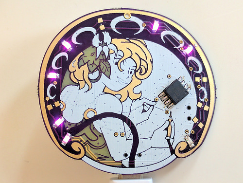
Liz from Blitz City DIY wrote about the process of designing a PCB ornament:

edited_p1070247_euwtkNp04o

Designing a PCB Ornament

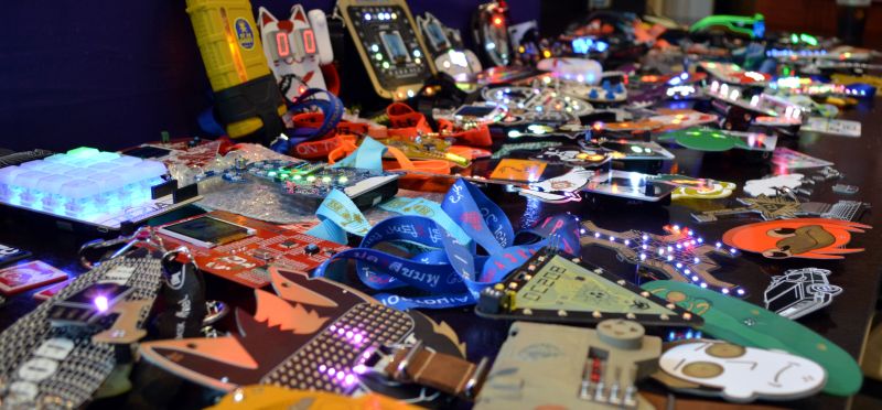
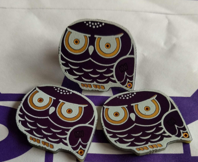
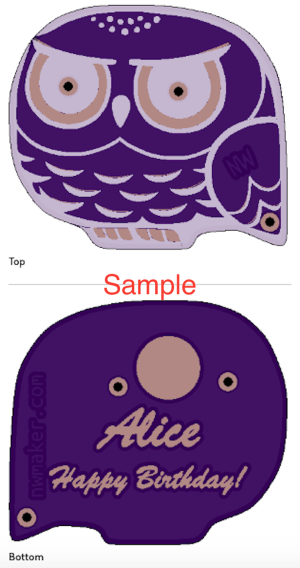
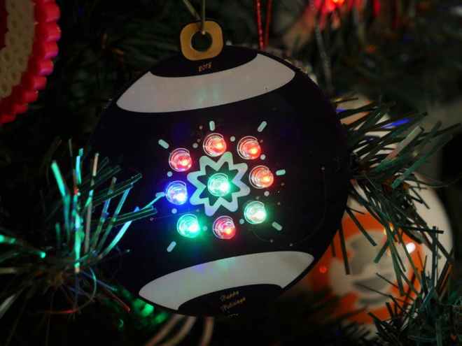
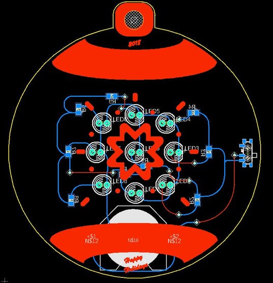
As the holidays approached this year, I felt a need to create a DIY gift for my family and friends. I struggled at first to find a medium. Should I 3D print something? Should I knit? But then it hit me: everyone loves blinky LEDs and I want to keep getting better at PCB design. I’ll do a PCB ornament!

orbornamentlayout_g9hVPwjRbg

If you don’t have a traditional electronics background PCB design can seem scary, overwhelming and something that’s meant for more experienced people that have “real skills”. If you start simple and slowly add-in new methods and design features to your boards you’ll soon realize it isn’t so scary and that much like everything else in life it just takes practice and patience to learn. And once you have your first project on a custom PCB instead of a piece of perf board you’ll be hooked.

Designing a PCB Ornament

Snowy Owl PCB artwork

A purple snowy owl with customizable name and short message from NWMaker on Tindie:

2018-08-20T00_35_36.935Z-purplesnowy3.png

Snowy Owl

Look at it. This snowy owl is so cute. You can choose add custom text or not.

When you choose the option of custom text, you can customize the snowy owl as follows.

  • Add a name or nick name (less than 16 letters) like “Mary” or “James”
  • Add a short message (less than 18 letters) such as “Happy Birthday!” or “Merry Christmas!”

2018-08-21T01_01_17.348Z-happy-verticalowl.png

Owl is amazing. It has super eyesight at night. Its feather structure makes its flight silent. It can turn around its head backwards.

I’d like something to be associated with “snow” and “north”. That is why I think of the snowy owl.

Snowy Owl PCB artwork

Kicad: Designing With Complex Shapes

Screenshot from 2018-07-10 11-57-36.png

KiCad presentation by Andrew Sowa at Teardown 2018:

Kicad: Designing With Complex Shapes

While most PCBs can be simple rectangles, sometimes the design requires more complex geometry. EDA tools don’t always make this simple, so we will go over a few KiCad tips to make it easier. In this talk you will learn how to import unique board shapes from Fusion 360, create arbitrary fill zones using images, and embed high-frequency RF filters. We will use multiple software packages to enhance KiCad’s performance beyond its obvious use.

Kicad: Designing With Complex Shapes

PCB projects with awesome artwork


Here’s a list of some project with great PCB artwork:

Pure art boards

Functional boards with awesome art/layouts

PCB projects with awesome artwork

Making Braille Signs out of PCBs

From  on Hackaday:

Screenshot from 2017-11-01 11-47-06.png

Making Braille Signs out of PCBs

[jg] recently passed some damaged Braille signs and took on the challenge of repairing them. Informed by his recent work on PCB lapel pins, [jg] immediately thought of using circuit boards for this project. He’d noticed that round solder pads made for uniform hills of solder, and this reminded him of the bumps in Braille.


He began by reading up on the standards of the Braille Authority of North America, which stipulates a dot height of 0.6mm. He loaded up the PharmaBraille font system and laid it out the dots in photoshop, then and imported it into KiCad and laid out the boards. When the PCBs had arrived from OSH Park, [jg] soldering up the pads (lead free, but of course) to see if he could get the hills to 0.6mm. He’s experimenting with different methods of melting the solder to try to get more even results


Making Braille Signs out of PCBs

Building a PCB lapel

JinGen Lim created this beautiful project:

csslapel-done

Building a PCB lapel

I had little experience with fabric, but building a lapel out of PCB seemed like something that might just work. PCBs are typically built with extremely high tolerances for its copper and mask layers and still acceptably accurate for the silkscreen.


Building a PCB lapel

PCB Artwork in 2017

Screenshot from 2017-06-26 19-46-18

wrote on Hackaday about the amazing PCB artwork that he’s seen so far in 2017:

Hackaday Links: June 11, 2017

PCB art is getting better and better every year.  This year, though, is knocking it out of the park.  In March, Andrew Sowa turned me into money.

screenshot-from-2017-03-23-13-54-53.png

More recently, Trammell Hudson has explored the layers of OSH Park soldermask and silk to create a masterpiece.

34937910986_9bdbb83edc.jpg

Now, we’re moving up to full-blown art. Blake Ramsdell worked with OSH Park to create a full panel of art in gold, fiberglass, soldermask, and silkscreen. It’s 22×16 inches, and it’s fantastic.

DB02l7LXoAIhTwL

David I. Herman just created a Facebook group for PCB paintings.

DC_ANixW0AEB2Fq

PCB Artwork in 2017