Jeremy S Cook writes about the experience of designing their first PCB:
Take the Plunge into PCB Design
While I’ve been experimenting with circuits for years, decades even, my projects tend to be filled with a rat’s nest of wires. These snake about with the constant possibility of disconnection or other problems. They are a pain both to assemble and troubleshoot. Breadboards and perfboards are one possible solution, but I don’t particularly enjoy working with them, and they also tend to be quite messy in my case.
A final possibility is the printed circuit board, with precise connections from point-to-point made by a machine. This seems like a great solution, but to someone who has never made one, it also seems like a black art—something pursued by people much more competent than myself.
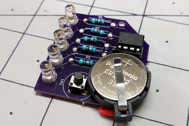
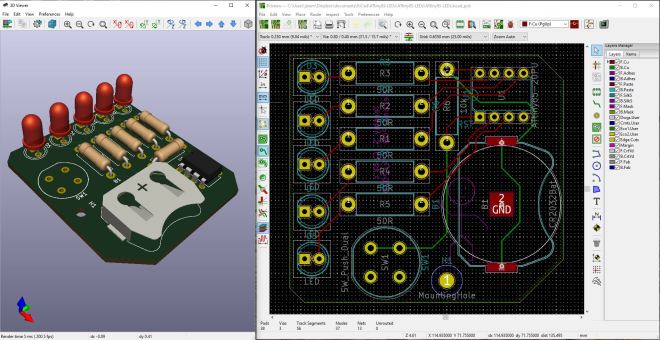
As someone that has recently designed two PCBs in the open-source KiCAD EDA platform, I know that this is not the case whatsoever. There is certainly a video tutorial out there somewhere to walk you through the process, this is what I recently used. I found these text instructions to be quite good, and going through it probably helped me remember things better.
