Cabe Atwell writes on Hackster about a RF filter adapter was made using some spare parts and lowpass and bandpass filter kits:
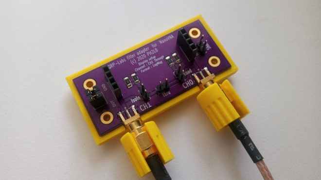
QRP-Labs Filter Adapter for NanoVNA
Check out Lex Bolkesteijn’s new project constructing a QRP-Labs filter adapter for NanoVNA with some spare parts and lowpass and bandpass filter kits. The NanoVNA is a tiny handheld Vector Network Analyzer (VNA), which accomplishes both high-performance and portability. Besides working as a vector network analyzer and antenna analyzer, this build utilizes it as a filter tuner.
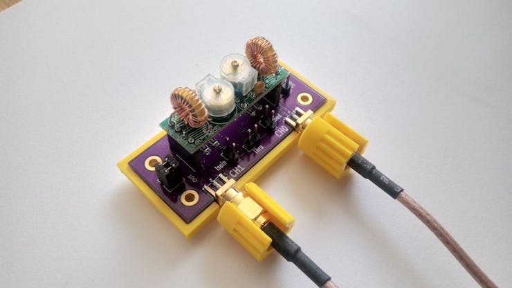
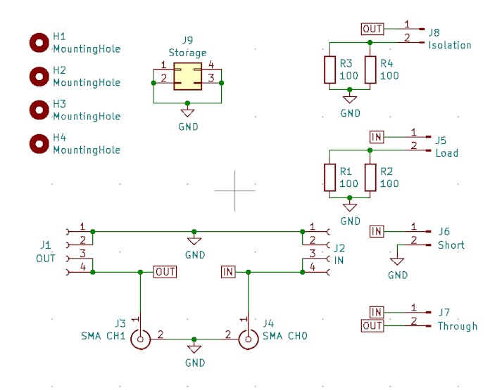
A current work in progress, last updated in mid-June, it was developed using a double-sided PCB, two SMA chassis, and a header cut in two to form a filter holder that enabled the use of the NanoVNA to test and tune the filters as required. The filter kits themselves include the double-sided PCD along with silkscreen, solder mask, and through-hole plating, as well as the capacitors. Both are the same size, and so require no adjustments to the filter holder.
Although the filter has four pins, five holes are drilled in the PCB base of the filter holder using a perforated PCB for spacing. The fifth hole allows for a via to connect the top and bottom layers. With some soldering, the via, SMA chassis parts, and headers are connected to the base. In a few steps that, everything is set up to connect the filter to the NanoVNA.
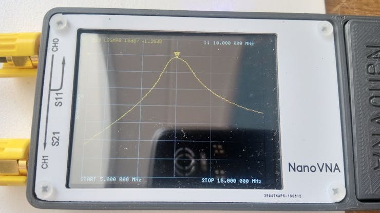
The NanoVNA should be calibrated before use, and in the documented project, this was done with an experimental calibration tool. When calibrating as close as possible to the adaptor, it’s not possible to use the calibration standards. The calibration tool was made with another PCD, with holes drilled for vias and two 100 Ohm SMD 1206 resistors.
A design, complete with CAD files for the casing, is also included for those who are unable to mill PCBs by hand. This uses a 3D-printed casing and custom-ordered PCBs to serve as the adapter. Simplifying the manual work required in the design, even more, the most recent custom PCB ordered includes built-in calibration options. The 3D-printed base looks spiffier than the hand-milled PCBs and requires no additional PCB for calibration.
For anyone interested, the bill of materials, CAD files, and a step-by-step with images are freely available on Bolkesteijn’s blog.