QRP-Labs Filter Adapter for NanoVNA

Cabe Atwell writes on Hackster about a RF filter adapter was made using some spare parts and lowpass and bandpass filter kits:

nanovna_qrplabs_20_FEE8nQ8TSv

QRP-Labs Filter Adapter for NanoVNA

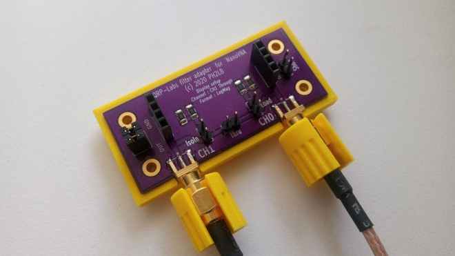
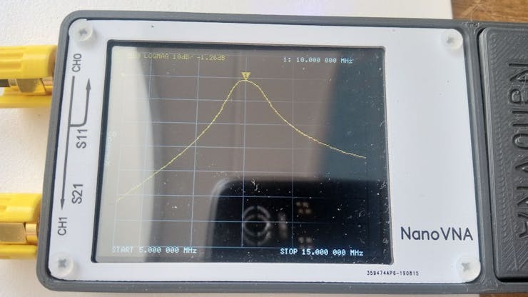
Check out Lex Bolkesteijn’s new project constructing a QRP-Labs filter adapter for NanoVNA with some spare parts and lowpass and bandpass filter kits. The NanoVNA is a tiny handheld Vector Network Analyzer (VNA), which accomplishes both high-performance and portability. Besides working as a vector network analyzer and antenna analyzer, this build utilizes it as a filter tuner.

A current work in progress, last updated in mid-June, it was developed using a double-sided PCB, two SMA chassis, and a header cut in two to form a filter holder that enabled the use of the NanoVNA to test and tune the filters as required. The filter kits themselves include the double-sided PCD along with silkscreen, solder mask, and through-hole plating, as well as the capacitors. Both are the same size, and so require no adjustments to the filter holder.

Although the filter has four pins, five holes are drilled in the PCB base of the filter holder using a perforated PCB for spacing. The fifth hole allows for a via to connect the top and bottom layers. With some soldering, the via, SMA chassis parts, and headers are connected to the base. In a few steps that, everything is set up to connect the filter to the NanoVNA.

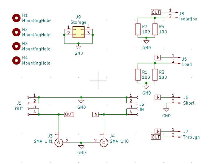
The NanoVNA should be calibrated before use, and in the documented project, this was done with an experimental calibration tool. When calibrating as close as possible to the adaptor, it’s not possible to use the calibration standards. The calibration tool was made with another PCD, with holes drilled for vias and two 100 Ohm SMD 1206 resistors.

A design, complete with CAD files for the casing, is also included for those who are unable to mill PCBs by hand. This uses a 3D-printed casing and custom-ordered PCBs to serve as the adapter. Simplifying the manual work required in the design, even more, the most recent custom PCB ordered includes built-in calibration options. The 3D-printed base looks spiffier than the hand-milled PCBs and requires no additional PCB for calibration.

For anyone interested, the bill of materials, CAD files, and a step-by-step with images are freely available on Bolkesteijn’s blog.

QRP-Labs Filter Adapter for NanoVNA

Build Your Own RF Lab: Scalar Network Analyzer

Whitney Knitter writes on Hackster about a simple scalar network analyzer that can be controlled by a Raspberry Pi for measuring the frequency response of filters and networks:

screen_shot_2020-06-21_at_12_39_16_am_QwvfFybZEx

Build Your Own RF Lab: Scalar Network Analyzer

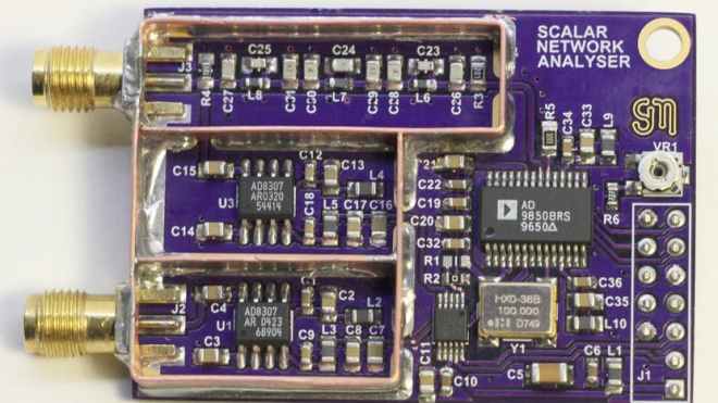
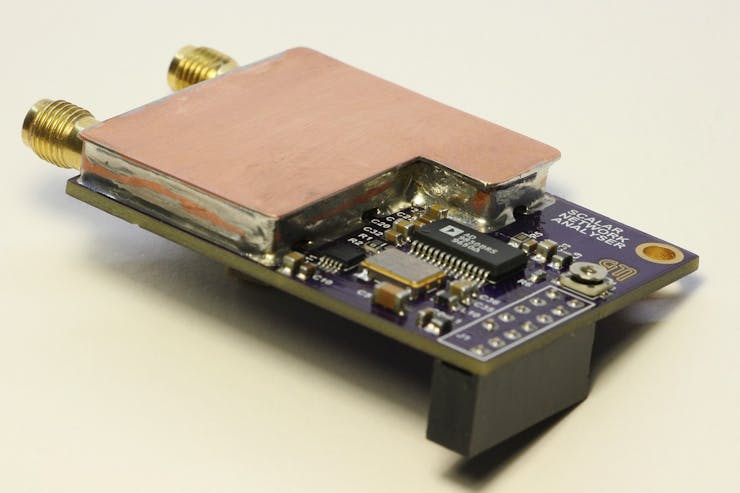
With the popularity of wireless applications having become such a staple in the hobbyist community, the need for RF testing capabilities in the hobbyist realm has also increased. Anyone familiar with traditional RF test equipment knows that it is expensive. But challenges like this are what bring out the engineering creativity in this community. Steven Merrifield designed and laid out his own simple scalar network analyzer (SNA) using just a few IC chips. SNAs are handy for testing the frequency response of filters or networks.

A scalar network analyzer is used to test the amplitude of a device’s frequency response by outputting a sine wave sweeping over a certain frequency range (bandwidth) then measuring the amplitude of each incremental output frequency.

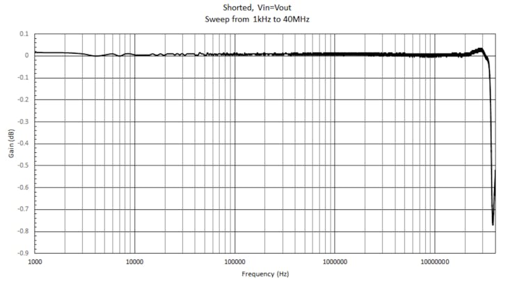
Thus if you directly connect the sine wave output of an SNA to its measurement input, then it will read a flat line of the same amplitude for each incremental output frequency of the sweep:

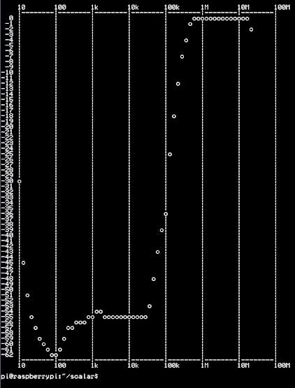
When a device is connected to the SNA, the amplitude of the sine wave at each frequency after going through the device will reflect the device’s frequency response over that bandwidth.

Merrifield’s design accomplishes an SNA’s functionality via implementation of a DDS Synthesizer chip, an ADC, and a logarithmic amplifier chip. The AD9850 DDS is responsible for outputting the sweeping sine wave while the AD8307 logarithmic amplifier conditions the signal input into the SNA for the log of the signal’s envelope before passing it on to the ADC for digitizing. A second AD8307 also conditions the output of the DDS and outputs it to a second channel of the ADC so that it can be used in software for compensation of any variations on the DDS’s output due to the effects of various loads of devices being tested.

The ADC outputs its digital measurements via an I2C interface to a GPIO header that matches the Raspberry Pi’s GPIO header pinout, but any desired MCU or FPGA could be used. The source code Merrifield wrote is in C, making it easy for porting across different platforms.

Check out Merrifield’s project logs here. He linked his PCB layout on OSH Park if you’re interested in ordering it and putting one of these together for your own lab!

Build Your Own RF Lab: Scalar Network Analyzer

QRP-Labs filter adapter for NanoVNA

nanovna_qrplabs_06

QRP-Labs filter adapter for NanoVNA

I had a few QRP-labs lowpass filters and bandpass filters kits laying around and because I had nothing better to do this afternoon, I fired up the soldering station and assembled them. After that they need to be tested and tuned.

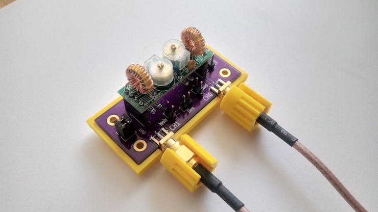
Owning a NanoVNA for a few months now (and hardly use it because for antenna stuff i use my RigExpert AA-600), I decided to use the NanoVNA for tuning the filters. So from some pieces out of my junkbox (a piece of double sided pcb, 2 sma chassis and a header cut in 2) I build this simple filter holder allowing me to test and tune the filters to my requirements.

Adding the 3D printed base plate, hooking it with my NanoVNA.

nanovna_qrplabs_06

Doing the calibration routine.

nanovna_qrplabs_06

And ready for testing.

nanovna_qrplabs_06

As expected like the previous design. But now no aditional PCB for calibration.

nanovna_qrplabs_06

Can only say that the purple on yellow looks cool 🙂

For those who want a adapter, checkout my ForSale page.

QRP-Labs filter adapter for NanoVNA

Hackaday Superconference: An Analog Engineer Dives Into RF

Those of us who work with electronics will usually come to the art through a particular avenue that we master while imbibing what we need from those around it. For example, an interest in audio circuitry may branch into DSP and microcontrollers as projects become more complex. Some realms though retain an aura of impossibility, a reputation as a Dark Art, and chief among them for many people is radio frequency (RF). Radio circuitry is often surprisingly simple, yet that simplicity conceals a wealth of complexity because the medium does not behave in the orderly manner of a relatively static analogue voltage or a set of low-frequency logic levels.

Chris Gammell is a familiar face to many Hackaday readers for his mastery of much electronic trickery, so it comes as something of a surprise to find that RF has been one of the gaps in his knowledge. In his talk at the Hackaday Superconference he took us through his journey into RF work, and the result is a must-watch for anyone with a curiosity about radio circuitry who didn’t know where to start.

via Hackaday Superconference: An Analog Engineer Dives Into RF — Hackaday

Quote

Weird World of Microwaves Hack Chat

Join us on Wednesday, December 18 at noon Pacific for the Weird World of Microwaves Hack Chat with Shahriar Shahramian! We’ve been following him on The Signal Path for years and are excited to pick his brain on what is often considered one of the dark arts of electronics.

No matter how much you learn about electronics, there always seems to be another door to open. You think you know a thing or two once you learn about basic circuits, and then you discover RF circuits. Things start to get a little strange there, and stranger still as the wavelengths decrease and you start getting into the microwave bands. That’s where you see feed lines become waveguides, PCB traces act as components, and antennas that look more like musical instruments.

via Weird World of Microwaves Hack Chat — Hackaday

Quote

Hackaday Prize Entry: Sub Gigahertz RF

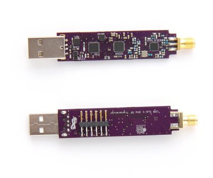
For his Hackaday Prize entry, [Adam] is working on an open source, extensible 915 and 433 MHz radio designed for robotics, drones, weather balloons, and all the other fun projects that sub-Gigaherts radio enables.

The design of this radio module is based around the ADF7023 RF transceiver, a very capable and very cheap chip that transmits in the usual ISM bands. The rest of the circuit is an STM32 ARM Cortex M0+, with USB, UART, and SPI connectivity, with support for a battery for those mobile projects.

via Hackaday Prize Entry: Sub Gigahertz RF — Hackaday

Hackaday Prize Entry: Sub Gigahertz RF

Mesh networking for sensor grids

Mesh networking board by Daniel on Hackaday.io:

5170671492304948896.jpg

Low-power mesh networking for small sensor grids

Tiny MQTT-interoperable broadcast mesh networking with simple radios

This project is a low-resource mesh networking stack and mote with battery-powered routers based on state synchronization. The target is for the stack to use less than 2kb SRAM. Nodes use low power listening and an adaptive gossip protocol to synchronize key/values pairs with each other without relying on explicit routing or per-node addressing.

5731331492306797027.png

For example, a light might transmit (/lamp, {“state”:”on”}) to the mesh. Write (/lamp, {“state”:”off”}) to the mesh, and the lamp application will notice. The powerful but simple state synchronization primitive allows you to update the state of the mesh to update the world, and update the state of the world to express the same on the mesh. Trivially bridged to a private MQTT server and managed with off-the-shelf MQTT applications.

The design files and source code are available on Bitbucket:

dholth/mesh

Mesh networking for sensor grids

Pidgeon 1 Sub-GHz Radio

Pidgeon 1 on Crowd Supply is a sub-GHz radio with 500 mW transmission power, RS485 networking interface and a STM32F0 microcontroller:
front-and-back_jpg_project-body

Crowd Supply: Pidgeon 1

No more restrictions from high level software! Access the lowest level of digital radio transmission with this programmable sub-GHz wireless module.

Hardware Specifications:

  • Radio – CC1120 + CC1190
  • Controller – STM32F051K6
  • FTDI USB interface – FT234XD-R
  • RS485 interface – LTC2850IDD
  • Buck converter – RT8010GQW
  • SMA connector for antenna
Pidgeon 1 Sub-GHz Radio

DTV Tuner Breakout for SDR

Eric Brombaugh designed this breakout board for the Rafael Microelectronics R820T2 Advanced Digital TV Silicon Tuner chip:

r820t2_breakout_assembled

R820T2 Breakout

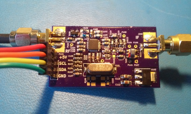
This is the same chip used in most all of the RTL-SDR dongles, as well as the Airspy and numerous other radios. The chip is a versatile front-end with reasonable sensitivity and wide tuning range.

screenshot-at-2017-02-17-13-54-36

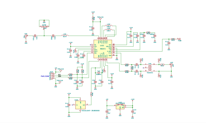
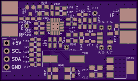
The design presented here is almost an exact implementation of the Mfg’s suggested demo design from the datasheet, implemented on the OSHpark 4-layer PCB process and provides a simple 4-pin interface with power, ground and I2C bus for controlling the tuner. A broad-band RF input and 10MHz IF output are provided on SMA connectors.

The breakout PCB design and STM32F0 firmware for the Rafael R820T2 tuner chip are shared on GitHub:

screenshot-at-2017-02-14-20-58-40 emeb/r820t2


emeb has shared project on OSH Park:

r820t2_breakout v0.1

cd102a38f8c39fe1ff2d6fe4cfe90e12.png
Order from OSH Park

DTV Tuner Breakout for SDR

PCB Design Guidelines to Minimize RF Transmissions

screenshot-at-2017-01-27-10-24-11

 writes on Hackaday:

PCB Design Guidelines to Minimize RF Transmissions

There are certain design guidelines for PCBs that don’t make a lot of sense, and practices that seem excessive and unnecessary. Often these are motivated by the black magic that is RF transmission. This is either an unfortunate and unintended consequence of electronic circuits, or a magical and useful feature of them, and a lot of design time goes into reducing or removing these effects or tuning them.

You’re wondering how important this is for your projects and whether you should worry about unintentional radiated emissions [..]

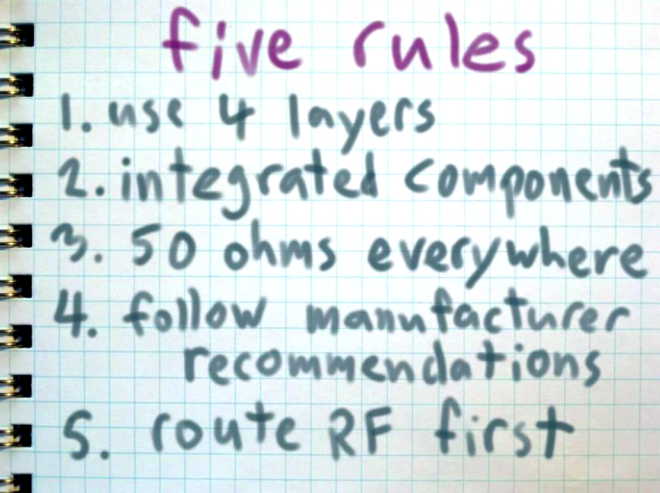
Another good guide is Michael Ossmann’s simple RF design rules:

five_rules.png


PCB Design Guidelines to Minimize RF Transmissions