Kicad: Designing With Complex Shapes

Screenshot from 2018-07-10 11-57-36.png

KiCad presentation by Andrew Sowa at Teardown 2018:

Kicad: Designing With Complex Shapes

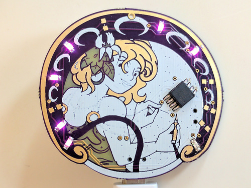
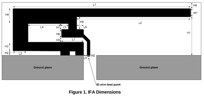
While most PCBs can be simple rectangles, sometimes the design requires more complex geometry. EDA tools don’t always make this simple, so we will go over a few KiCad tips to make it easier. In this talk you will learn how to import unique board shapes from Fusion 360, create arbitrary fill zones using images, and embed high-frequency RF filters. We will use multiple software packages to enhance KiCad’s performance beyond its obvious use.

Kicad: Designing With Complex Shapes

Building a Giant USB Three Key Mechanical Keyboard

From Jeremy S. Cook on the Hackster blog:

1_Un7UKnIW5LinAhX8Pbg4DQ

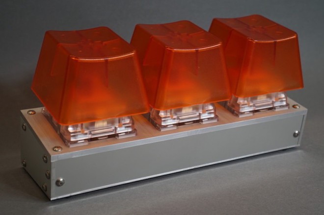
Ginormous 3-Switch Keyboard Is Awesomely Impractical

As hackers and creators, we sometimes get asked the question “why?” While many of the gadgets we make do have a specific purpose, many of them definitely don’t, and are made because we wonder if something can actually be done. This giant three-key mechanical keyboard would certainly fall into that second category, and though I can’t think of a practical use for it, I still find the device quite entertaining.

1_nDZswgG0dfI2lgmY9SzFFw

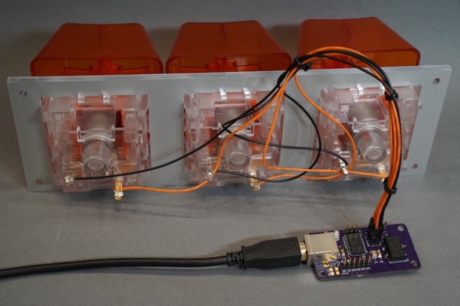
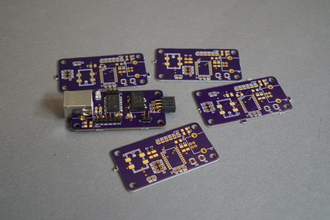
The heart of this device is a trio of “Big Switch” devices from Novel Keys, which are four times larger in length/width/height than what you’re used to typing on. While that might sound only sort of interesting, that translates to 64 times normal size in volume; plus they include similarly ginormous keycaps. Glen Akins, inspired by a similar project on Adafruit, decided to build his own 3-key array, with a PIC18F14K50 chip providing an interface between the keys ans USB input.

DSC00640-1024x683.jpg

The housing is made out of aluminum, and sits at an angle to the user for excellent ergonomics — if you happen to be a giant, and only use three keys at a time. While the electronics are fairly straightforward, these large keys are electrically quite noisy. Debounce code was added to combat this, reducing the letters per keypress from a range of one to three to only a single character.

Read more on Glen’s own Photons, Electrons, and Dirt blog:

Building a Giant USB Three Key Mechanical Keyboard

Building a Giant USB Three Key Mechanical Keyboard

PCB Artwork in 2017

Screenshot from 2017-06-26 19-46-18

wrote on Hackaday about the amazing PCB artwork that he’s seen so far in 2017:

Hackaday Links: June 11, 2017

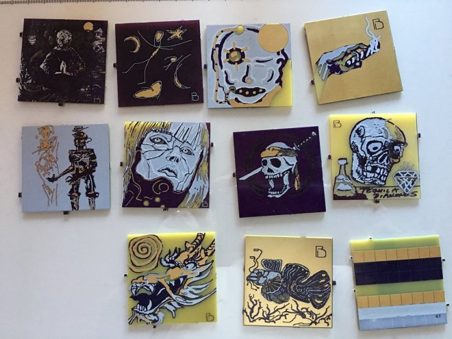
PCB art is getting better and better every year.  This year, though, is knocking it out of the park.  In March, Andrew Sowa turned me into money.

screenshot-from-2017-03-23-13-54-53.png

More recently, Trammell Hudson has explored the layers of OSH Park soldermask and silk to create a masterpiece.

34937910986_9bdbb83edc.jpg

Now, we’re moving up to full-blown art. Blake Ramsdell worked with OSH Park to create a full panel of art in gold, fiberglass, soldermask, and silkscreen. It’s 22×16 inches, and it’s fantastic.

DB02l7LXoAIhTwL

David I. Herman just created a Facebook group for PCB paintings.

DC_ANixW0AEB2Fq

PCB Artwork in 2017

Designing PCBs for Assembly

Designing pcbs for assembly is easy, right? We just squirt all the footprints onto a board layout, connect all the traces, send out the gerbers and position files, and we’re done–right? Whoa, hold the phone, there, young rogue! Just like we can hack together some working source code with variables named after our best friends, we can also…

via Designing for Fab: a Heads-Up before Designing PCBs for Professional Assembly — Hackaday

Designing PCBs for Assembly

KiCAD Best Practices: Library Management

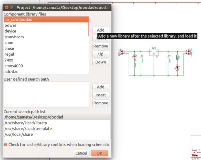
One common complaint we hear from most new KiCAD users relates to schematic and footprint libraries. The trick is to use just one schematic symbol and footprint library each with your project. This way any changes to the default schematic libraries will not affect your project and it will be easy to share your project with others without breaking…

via KiCAD Best Practices: Library Management — Hackaday

eeschema_lib.png

KiCAD Best Practices: Library Management

Robotic Arts: Noodle is Gettin’ Bean Feet

Sarah Petkus posts an update on her Robotic Arts blog about her NoodleFeet robot:

Noodle is Gettin’ Bean Feet!

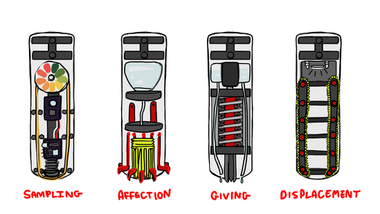
This summer, I am once again diving into designing mechanical personality quirks. I’ll be investigating new and exciting ways for my robot, NoodleFeet to interact with the world. This time, my focus is the wet, tingly and preferential aspect of TASTE.

moduledrawings

From now until the end of August, my goal is to produce four different tasting modules that each demonstrate some aspect of sampling or preference. You could think of them as the “four tasters of the apocalypse”

If you’re unfamiliar with Sarah and NoodleFeet, then check out here great talk from Hackaday Super Con:

Robotic Arts: Noodle is Gettin’ Bean Feet

Protosnap

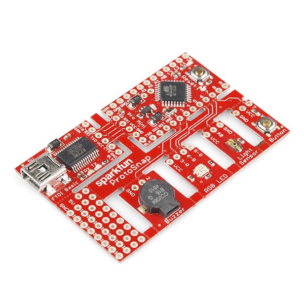
We’re huge fans of Sparkfun’s old school ProtoSnap kits. These include a small support tab with traces running between different sections of the board. They’re great for kit designs, allowing for both immediate out-of-box functionality, and eventual customization.

0lsnm_br3taavxnql
Due to our shipping and panelization process, this type of board is not fully supported, but can be fabricated with careful consideration and experimentation.

Design Considerations

These designs are almost always unique, since the number of shapes, sizes, and orientation varies wildly. The design also may need adjusting based on the intended user.

in orientation, intended usage, and shape. As a result, a bit of experimentation is always going to be required. However, here’s a few design tips to get things going.

  • Always ensure that after snapping, you can connect the boards together easily. A small header pinout near the tab works most of the time, but some designs might work best with a special connector.
  • Tab width is critical. If the tab is too narrow, it will not hold the board together well. Too wide, and it becomes difficult to break apart. 3-5 trace/hole pairs works best.
  • Hole size / pitch. The best tabs have between 20-30 mil of material between the holes. A hole size of 25 mil generates pretty good tabs.
  • Design permitting, having multiple tabs with 2-3 holes is better than one huge tab with 6 or more connections.
  • Adding traces on both top and bottom of a tab is likely to result in difficult snapping. Consider instead using more tabs, or adding instructions to score the traces.
  • Tab and board placement: Remember that your users has to remove these! If the boards are badly positioned, the tabs aren’t “snapped” as much as they are “twisted”. This can result in unusual failures.

Designing for Failures

Since these typically are for kits, the most likely failure that will occur is a pulled up trace. This is when the trace on the two boards doesn’t break, and starts pulling up traces inside your layout. Not good. Fortunately, the design can account for this in several ways.

Any of these techniques will generate a “stress concentration point” for a pulled up trace. This will cause a the trace to tear in a well-defined place, ensuring that it won’t affect your board.

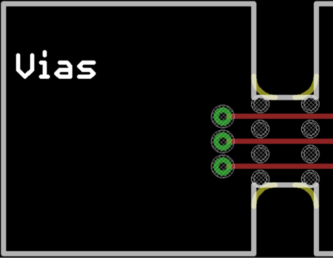
The simplest one simply having vias near the tab, as seen on the sparkfun board above. A ripped up trace will usually break at the edge of the via pad.

0u2dr3nu2dsf7ip8_

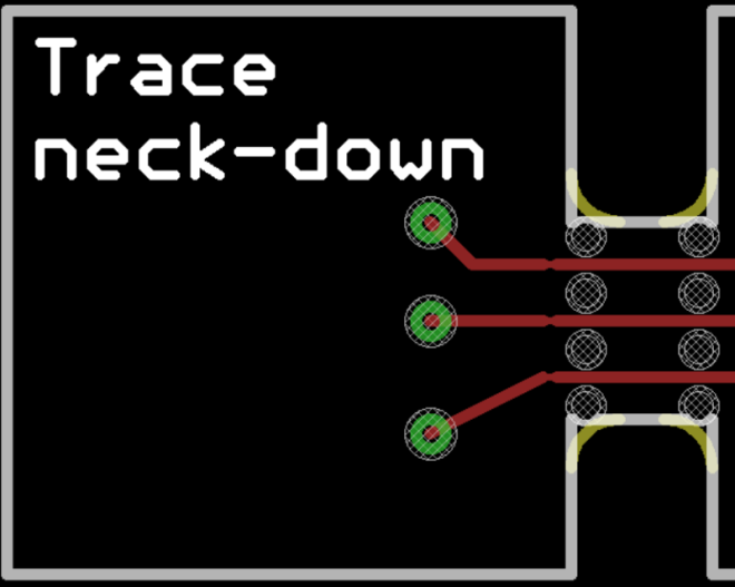
Another option is to actually narrow the trace near the board edge. This takes up less space than a via, but still provides a good weak point in a desirable location. However, make sure you don’t go too far below the design rules!

0-_q8d8anjviisrqn

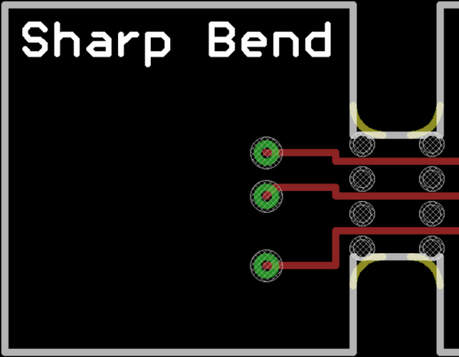
The last option is less ideal, but may suit certain layouts. Simply jog the trace, creating a 90° bend or two.

0pqpeob5lt4fobxon

Indicating on the design

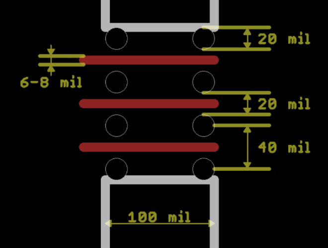
Here’s the measurements on our typical support tabs. Your design may require different configurations, so these are a rough guideline.

Typical tabs have the following features

  • 20-25 mil drill hits
  • 20-25 mil between the edge of the drilled holes
  • roughly a 40 mil drill pitch
  • 2-5 holes per tab (3-4 recommended)
  • Holes tangent to the original board outlines
0cftx3ethihgsbtlg

Note, the milling tool will add a 34 mil corner radius on the tabs. As a result, you can place the outermost holes tangent to the tab edge.

Failure modes (and how to cope)

  • Pulled up traces? Need to add a break closer to the edge, or score the board before snapping. Try to handle this on a design revision before a full kit.
Protosnap

PCB Design Guidelines to Minimize RF Transmissions

screenshot-at-2017-01-27-10-24-11

 writes on Hackaday:

PCB Design Guidelines to Minimize RF Transmissions

There are certain design guidelines for PCBs that don’t make a lot of sense, and practices that seem excessive and unnecessary. Often these are motivated by the black magic that is RF transmission. This is either an unfortunate and unintended consequence of electronic circuits, or a magical and useful feature of them, and a lot of design time goes into reducing or removing these effects or tuning them.

You’re wondering how important this is for your projects and whether you should worry about unintentional radiated emissions [..]

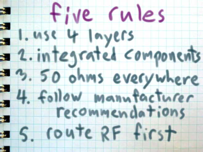
Another good guide is Michael Ossmann’s simple RF design rules:

five_rules.png


PCB Design Guidelines to Minimize RF Transmissions