Converting a vintage button panel to USB

Glen Akins (@bikerglen) writes about converting a vintage button panel to USB:

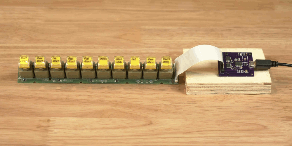
Converting a Vintage Grass Valley Button Panel to USB Using the Silicon Labs EFM8UB1

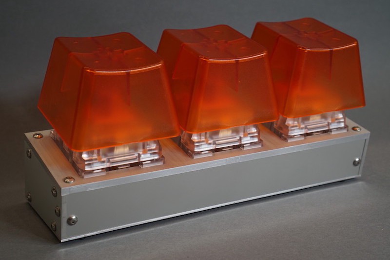
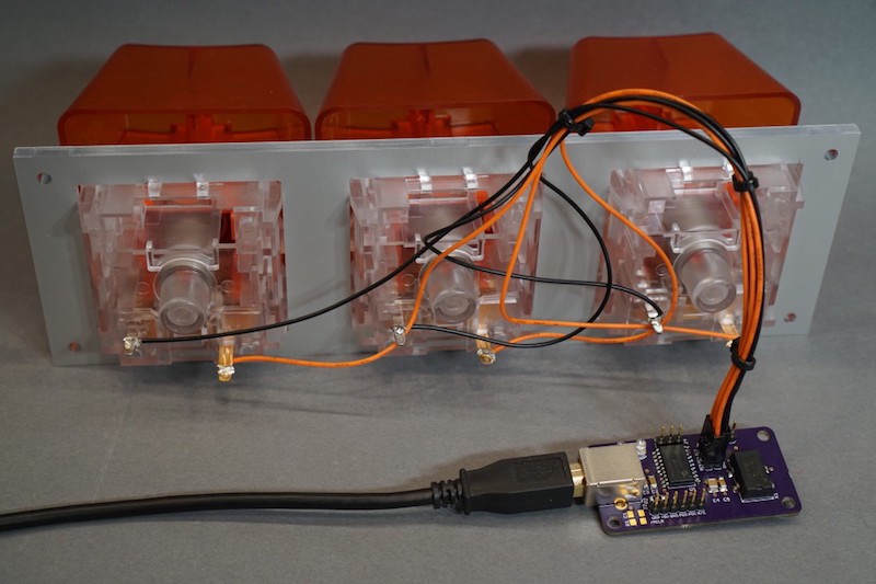
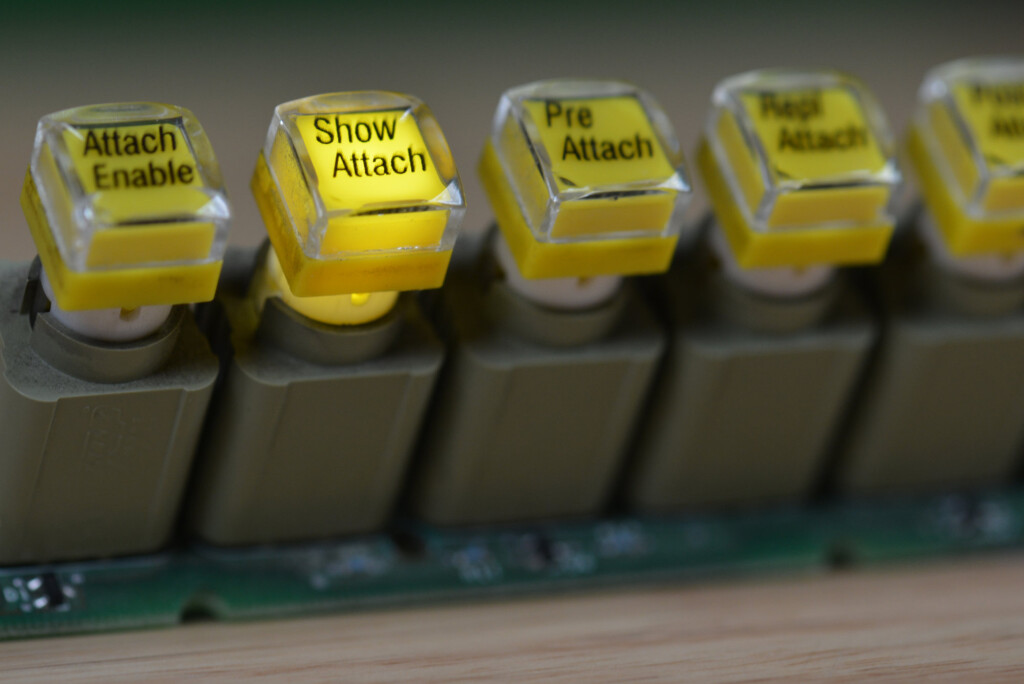
In this project, I convert a set of illuminated push buttons from a vintage Grass Valley video mixer into a custom vendor-defined USB HID peripheral. Like the USB analog panel meters project, this project uses a Silicon Labs EFM8UB1 microcontroller for USB connectivity. Unlike the panel meters project which only received data from the USB host, this project needs to send data back to the USB host too.

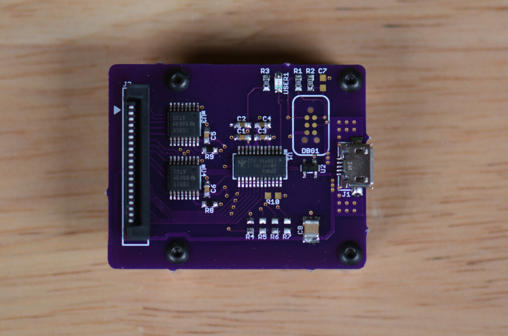
In this write up, we’ll reverse engineer the button panel, decide on a strategy for reading the keys and controlling the LEDs, build a board, then write both embedded and Linux software to interface with the button panel. If you want to build your own device like this but don’t have this specific switch panel, don’t worry–the ideas presented here are applicable to any generic 3×4/4×3/4×4 matrix keypad with or without LEDs.

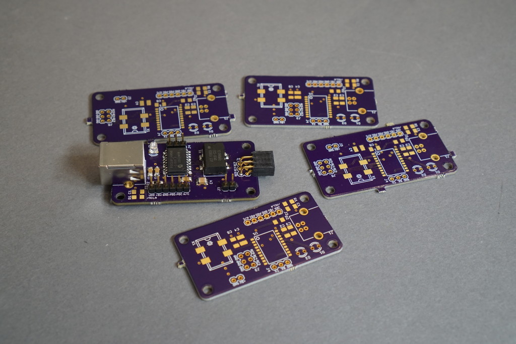
Design files for this project are in my usb-led-switch-matrix repository on GitHub.

Converting a vintage button panel to USB

Penguino Feather SAMR34 LoRa Dev-Board

Orkhan AmirAslan on Hackaday.io has created a RAK4260 based, Feather styled LoRa dev-board:

811081576236264418

Penguino Feather SAMR34 LoRa Dev-Board

This is a SAMR34 based LoRa dev-board with all the necessary components for fast prototyping. It’s a successor of my previous Penguino RF module and Feather breakout design ( https://www.tindie.com/products/16985/ )The new design uses the RAK4260 module from @RAKWireless and improves on some aspects, such as USB Type-C, RGB LED, user button, battery protection & voltage supervision, and optional flash & per-provisioned secure element IC pads.

Background:

About a year ago, after I first saw SAMR34 System in Package (SiP) in 2018 Electronica I couldn’t find a module for it and I took up the challenge for myself to build one myself. Then sharing first renders with the Twitterverse it gathered quite a bit of interest and I started selling couple over at my Tindie store. At the time I named the project TinyLoRa but for legal reasons I had to change it to Penguino.

Specs:

  • ATSAMR34J18 LoRA System-in-Package (SiP) based RAK4260
  • ARM Cortex M0+ MCU & SX1276 LoRa Radio
  • 256KB Flash, 40 KB RAM
  • Max Tx Power: +20 dBm; Max Sensitivity: -148dBm; Rx Current: 17mA (typical)
  • Frequency Range: 862 to 1020 MHz (DS values)
  • Deep Sleep Current: ~1 μA (module only)
  • Li-Po battery charging IC
  • RGB user LED, Battery Charge Status (red) and Power (blue) (w/ cut-off jumpers)
  • 3.3V low Iq LDO (~1 μA)
  • Low-voltage battery cut-off supervisor IC (3V Vbat cutoff)
  • USB Type-C connector with protection/filtering circuit
  • 0.75 A resettable fuse
  • Voltage divider for Vbat monitoring (w/ cut-off jumpers)
  • SMA and u.FL antenna connectors
  • 10-pin SWD programming header
  • Dimensions: 2 in. x 0.9 in. (50.8 mm x 22.8 mm)

Penguino Feather SAMR34 LoRa Dev-Board

Designing a PCB Ornament

Liz from Blitz City DIY wrote about the process of designing a PCB ornament:

edited_p1070247_euwtkNp04o

Designing a PCB Ornament

As the holidays approached this year, I felt a need to create a DIY gift for my family and friends. I struggled at first to find a medium. Should I 3D print something? Should I knit? But then it hit me: everyone loves blinky LEDs and I want to keep getting better at PCB design. I’ll do a PCB ornament!

orbornamentlayout_g9hVPwjRbg

If you don’t have a traditional electronics background PCB design can seem scary, overwhelming and something that’s meant for more experienced people that have “real skills”. If you start simple and slowly add-in new methods and design features to your boards you’ll soon realize it isn’t so scary and that much like everything else in life it just takes practice and patience to learn. And once you have your first project on a custom PCB instead of a piece of perf board you’ll be hooked.

Designing a PCB Ornament

Creating a DIP ATtiny85 Watch with the DS3231

Untitled drawing

Creating a DIP ATtiny85 Watch with the DS3231

As Douglas Adams explained in The Hitchhiker’s Guide to the Galaxy, digital watches are “pretty neat” to us primitive life forms. Something about the marriage of practicality, and sheer nerdiness gets me oddly excited. Somewhere in my fascination I asked myself, “can I make a digital watch entirely of my design?” I did! And it taught me a lot about pcb fabrication, low power programming, and shift registers.

ezgif.com-crop

Probably the most important function of a watch is that it keeps time. While you could use your microcontroller to count the seconds and save on parts, there are some major downsides to this. For one, the microcontroller is much worse at keeping time than a dedicated RTC (Real Time Clock) IC, the time would drift significantly with temperature and battery voltage. Another serious problem is that it would require the microcontroller to always be on, keeping track of the time. This would consume much more current than an RTC IC, draining the battery significantly faster. Thus we employ a DS3231 to casually sit in the background, consuming microamps from it’s own back-up battery (which, at the rate of 200µA, would take 12.56 years to drain).

Creating a DIP ATtiny85 Watch with the DS3231

Reflowduino: Put That Toaster Oven To Good Use

From  on the Hackaday blog:

Reflowduino: Put That Toaster Oven To Good Use

There are few scenes in life more moving than the moment the solder paste melts as the component slides smoothly into place. We’re willing to bet the only reason you don’t have a reflow oven is the cost. Why wouldn’t you want one? Fortunately, the vastly cheaper DIY route has become a whole lot easier since the birth of the Reflowduino – an open source controller for reflow ovens.

This Hackaday Prize entry by [Timothy Woo] provides a super quick way to create your own reflow setup, using any cheap means of heating you have lying around. [Tim] uses a toaster oven he paid $21 for, but anything with a suitable thermal mass will do. The hardware of the Reflowduino is all open source and has been very well documented – both on the main hackaday.io page and over on the project’s GitHub.

sidekick-e1525981389910

The board itself is built around the ATMega32u4 and sports an integrated MAX31855 thermocouple interface (for the all-important PID control), LiPo battery charging, a buzzer for alerting you when input is needed, and Bluetooth. Why Bluetooth? An Android app has been developed for easy control of the Reflowduino, and will even graph the temperature profile.

When it comes to controlling the toaster oven/miscellaneous heat source, a “sidekick” board is available, with a solid state relay hooked up to a mains plug. This makes it a breeze to setup any mains appliance for Arduino control.


Reflowduino: Put That Toaster Oven To Good Use

ATTiny wearable by Facelesstech

tl;dr It’s a foundation for a wearable platform. It’s a Nato watch strap threaded through a PCB with a coin cell battery holder between the PCB and the strap. I’m using a Attiny85 this time around but could be used for most chips/dev boards. This is a proof of concept to iron out any problems […]

via Attiny wearable — Facelesstech

ATTiny wearable by Facelesstech

Building a Giant USB Three Key Mechanical Keyboard

From Jeremy S. Cook on the Hackster blog:

1_Un7UKnIW5LinAhX8Pbg4DQ

Ginormous 3-Switch Keyboard Is Awesomely Impractical

As hackers and creators, we sometimes get asked the question “why?” While many of the gadgets we make do have a specific purpose, many of them definitely don’t, and are made because we wonder if something can actually be done. This giant three-key mechanical keyboard would certainly fall into that second category, and though I can’t think of a practical use for it, I still find the device quite entertaining.

1_nDZswgG0dfI2lgmY9SzFFw

The heart of this device is a trio of “Big Switch” devices from Novel Keys, which are four times larger in length/width/height than what you’re used to typing on. While that might sound only sort of interesting, that translates to 64 times normal size in volume; plus they include similarly ginormous keycaps. Glen Akins, inspired by a similar project on Adafruit, decided to build his own 3-key array, with a PIC18F14K50 chip providing an interface between the keys ans USB input.

DSC00640-1024x683.jpg

The housing is made out of aluminum, and sits at an angle to the user for excellent ergonomics — if you happen to be a giant, and only use three keys at a time. While the electronics are fairly straightforward, these large keys are electrically quite noisy. Debounce code was added to combat this, reducing the letters per keypress from a range of one to three to only a single character.

Read more on Glen’s own Photons, Electrons, and Dirt blog:

Building a Giant USB Three Key Mechanical Keyboard

Building a Giant USB Three Key Mechanical Keyboard

iceRadio SDR project

Software Defined Radio (SDR) project by Eric Brombaugh:
iceRadio.jpg

iceRadio

This is a test prototype for experimenting with Software Defined Radio (SDR). It is composed of several boards that are described in detail elsewhere on this site:

Combined with suitable firmware and FPGA design, these boards comprise a receiver capable of capturing 20kHz of signal from DC to over 1GHz, demodulating it with a variety of formats and driving high-quality audio.

iceRadio_system.png

Tuner

RF input from the antenna can optionally be tuned down from VHF/UHF frequncies to an IF frequency in the HF range before passing to the ADC.

ADC

Raw HF or downconverted VHF at an IF of 5MHz is digitized to 14-bit resolution. The maximum input signal allowed without exceeing the range of the ADC puts the 0dBfs point of this system at -10dBm in 50 ohms. The ADC runs at 40MSPS with a resolution of 10 bits, providing approximately 60dB of dynamic range and 20MHz of bandwidth which places the quantization noise floor at about -70dBm.

FPGA

From the ADC, data passes into the FPGA. This is an iCE5LP4k part which provides 20 4kb RAM blocks and 4 16×16 MAC blocks which are essential for the DSP required for the downconversion. In the FPGA the ADC data is pre-processed to a sample rate appropriate for the MCU. Figure 2 below shows the primary components of the FPGA design.

iceRadio_fpga

The C and Verilog source code is available on GitHub:

emeb/iceRadio

iceRadio SDR project