Matthew Venn has created a FPGA dev board based on Lattice iCE40 8k for the Raspberry Pi. The board uses our After Dark service which features clear solder mask on a black substrate:
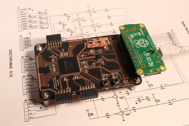
FPGA dev board based on Lattice iCE40 8k
Aim
- Make my first PCB with an FPGA
- Keep it super simple and cheap
- Configured by on-board FLASH or direct with a Raspberry Pi
- 6 PMODs, 2 buttons, 2 LEDs, FLASH for configuration bitstreams.
What a Lattice iCE40 FPGA needs
- A clock input. Has to be provided by an oscillator, it doesn’t have a crystal driver.
- 1.2v core supply for the internal logic.
- 2.5v non volatile memory supply. Can be provided via a voltage drop over a diode from 3.3v.
- IO supply for the IO pins, different banks of IO can have different supplies. This design uses 3.3v for all banks.
- Get configured over SPI interface. This can be done directly by a microcontroller or a computer, or the bitstream can be programmed into some FLASH, and the FPGA will read it at boot. If FLASH isn’t provided then the bitstream needs to be programmed at every power up or configuration reset.
- Decoupling capacitors for each IO bank.
PCB
- Schematic
- OHSPark project or Gerbers
- Cheap, 2 layer board. Probably not so good for fast signals.
BOM
- FPGA iCE40-HX4K-TQ144 (8k accessible with Icestorm tools)
- 3.3v reg TLV73333PDBVT
- 1.2v reg TLV73312PDBVT
- 12MHz oscillator SIT2001BI-S2-33E-12.000000G
- 16MB FLASH IS25LP016D-JBLE (optional).
Test
See the test program. This makes a nice pulsing effect on LED2, and LED1 is the slow PWM clock. The buttons increase or decrease pulsing speed.
make progYosys and NextPNR are used to create the bitstream and then it’s copied to the Raspberry Pi specified by PI_ADDR in the Makefile.
Fomu-Flash is used to flash the SPI memory, or program the FPGA directly.
