We are excited to see the wonderful Thomas Flummer in Copenhagen has designed a neat PCB pin for the virtual Chaos Communication Congress next month:
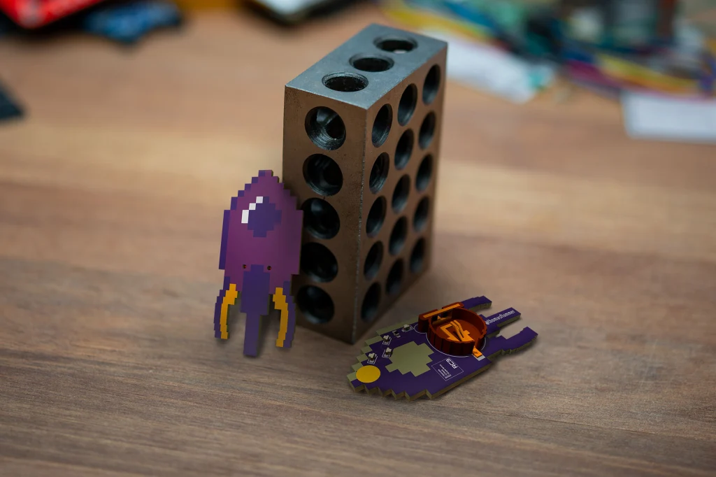
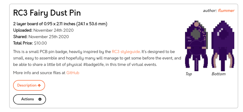
Fairy Dust mini PCB pin for RC3
This is a small PCB pin badge, heavily inspired by the RC3 styleguide. It’s designed to be small, easy to assemble and hopefully many will manage to get some before the event, and be able to share a little bit of physical #badgelife, in this time of virtual events.
Making your own
If you want to make your own, I have included the gerbers, in case you don’t want to install the nightly version of KiCad.
There is also a shared projects at OSHPark, and this is designed for the standard purple PCBs. It’s designed to be exactly 2 square inches, so for USD 10 you get 3 pcs. shipped anywhere, though the standard shipping might take a bit to arrive.
The parts needed for this pin is simply 4 white 0603 LEDs, a series resistor, also 0603, to limit the current a bit (I’ll try with a 1K to begin with), a CR1220 coin cell holder (I’m planning on using a Q&J CR1220-2 from LCSC) and then a little round brooch clasp/tie tack pin (I got some on ebay, but a DIY/craft supply store might also have them).
Please share
If you decide to make this badge or a variant of it, please share images so we can all see it and get inspired. If sharing on social media, please use the #badgelife tag and please let me know, I would love to see what you have made!
Here is the shared project: