Clever Wedges That Will Increase Your PCB Assembly Yield

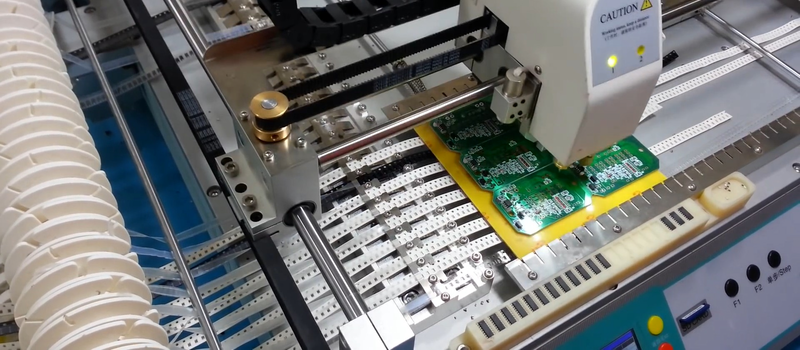
If there’s one thing that will bring down the yield of your PCB assembly, it’s your solder paste. Put too much on, and you’ll get bridged leads. If you don’t put enough on, that pad might not make good contact. [ScalarElectric] has an amazing trick that’s sure to astonish and astound. Just use wedges and you’ll get better yield with fine-pitched components.

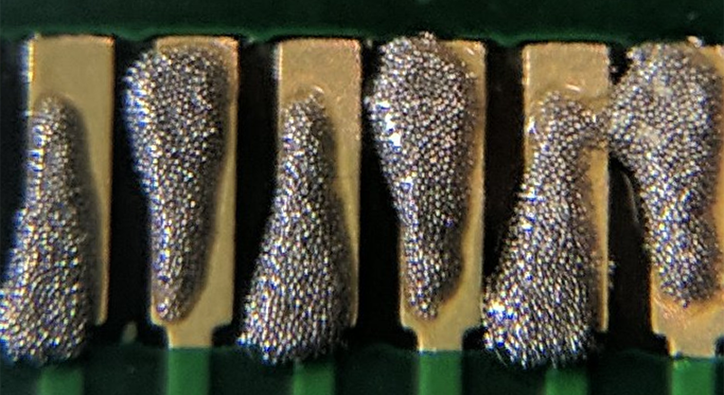
The trick here is to define the cream/solder paste layer of each package as a wedge on each pad instead of the usual rectangle. This gives a few benefits, the largest being the increased gap between paste shapes. You’re also getting a reduction in the total amount of paste applied, and a subsequent improvement in yield. (Reportedly, we’d love to see some data on this.)

via Clever Wedges That Will Increase Your PCB Assembly Yield — Hackaday

Quote

Advanced Assembly factory tour this Thursday (10/25)

Screenshot from 2018-10-17 13-55-33.png

If you’re in the Denver area, join Laen and Drew for an open house at our new assembly partner: Advanced Assembly!

Join us for pizza, beer and tours of our newly remodeled, high-tech facility as we celebrate 14 years in business. Bring your co-workers too!

Please RSVP

Screenshot from 2018-10-17 19-57-14.png

Advanced Assembly factory tour this Thursday (10/25)

Designing PCBs for Assembly

Designing pcbs for assembly is easy, right? We just squirt all the footprints onto a board layout, connect all the traces, send out the gerbers and position files, and we’re done–right? Whoa, hold the phone, there, young rogue! Just like we can hack together some working source code with variables named after our best friends, we can also…

via Designing for Fab: a Heads-Up before Designing PCBs for Professional Assembly — Hackaday

Designing PCBs for Assembly

OpenFixture Takes the Pain Out of Pogo Pins

test-fixture-featured

Hackaday reports:

OpenFixture Takes the Pain Out of Pogo Pins

[Elliot] wrote in with his OpenFixture model for OpenSCAD. It’s awesome because it takes a small problem, that nonetheless could consume an entire day, and solves it neatly. And that problem is making jigs to test assembled electrical products: a PCB test fixture.

aux_origin_button.png

In the PCB design software, you simply note down the locations of the test points and feed these into the OpenSCAD model.  [Elliot] shows you exactly how to do it using KiCAD. There are a few more parameters of the model that you can tweak to match your particulars, but you should have a DXF outline for a test jig in short order. Cut that out, assemble, and test.


OpenFixture Takes the Pain Out of Pogo Pins