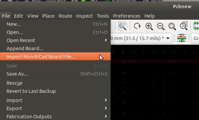
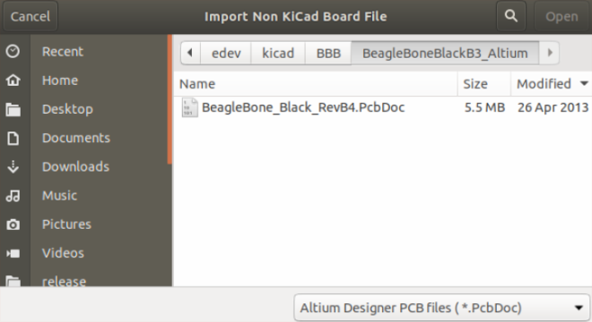
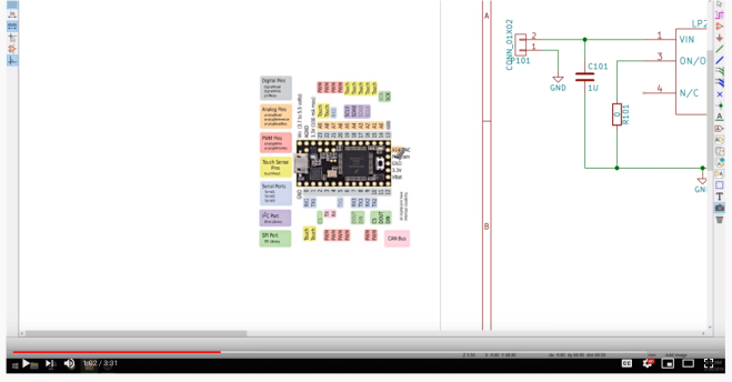
Thomas Pointhuber got Twitter excited yesterday with this video of importing Altium design into KiCad:
This is the foundation to add support for native Altium import. Contributions are very welcome, because this is a quite some amount of work.
The work is mainly based on https://github.com/thesourcerer8/altium2kicad, which is an existing Altium Designer -> KiCad converter written in Perl. Because Altium Circuit Studio and Altium Circuit Maker uses quite similar file formats, I try to support them as well in one go.
My current workflow is to try to understand the existing code, and build a binary documentation of the Altium format using Kaitai Struct. This allows fast iterations, and tells me if something is parsed incorrect.
CNX Software has a nice blog post on how to build the development version of KiCad:
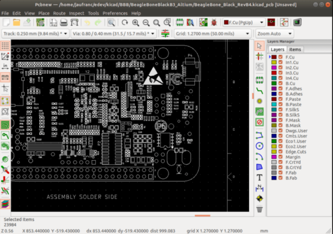
How to Build KiCad on Ubuntu 18.04 and Import Altium PCB Files
KiCad open-source EDA (Electronics Design Automation) suite software is now very popular, and many new projects are designed with the utility. AFAIK, some companies like Olimex switched all their new designs to KiCAD. But since many schematics and PCB layouts have been designed with other tools like EAGLE, Orcad Allegro, or Altium PCB design tools, it would be nice to be able to import those designs into KiCad.