In 2018, when KiCad Version 5 modernized the venerable 4.X series, it helped push KiCad to become the stable and productive member of the open source EDA landscape that we know today. It has supported users through board designs both simple and complex, and like a tool whose handle is worn into a perfect grip, it has become familiar and comfortable. For those KiCad users that don’t live on the bleeding edge with nightly builds it may not be obvious that the time of version 6 is nearly upon us, but as we start 2021 it rapidly approaches. Earlier this month [Peter Dalmaris] published a preview of the changes coming version 6 and we have to admit, this is shaping up to be a very substantial release.
Don’t be mistaken, this blog post may be a preview of new KiCad features but the post itself is extensive in its coverage. We haven’t spent time playing with this release yet so we can’t vouch for completeness, but with a printed length of nearly 100 pages it’s hard to imagine [Peter] left anything out! We skimmed through the post to extract a few choice morsels for reproduction here, but obviously take a look at the source if you’re as excited as we are.
I thought many would be interested in the development status and new features of pre-v6/post-v5 now when 5.1.0 has been released and version 6 development has begun. Add your favorite here if someone else hasn’t done it already.
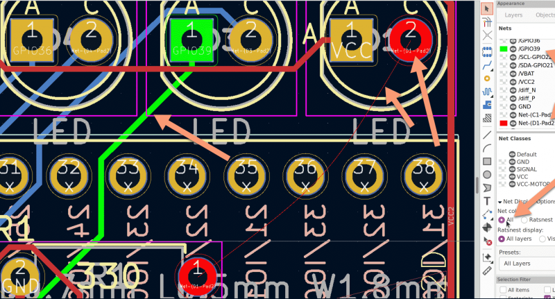
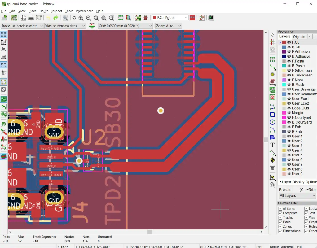
Routing differential pair lines in PCB layout software can be a tricky process. Luckily, KiCad has a few tools to help us with the process. In this tutorial, we’ll walk you through the process of calculating the differential impedance and using that information to create a pair of USB data lines in a project.
In this workshop, Anool Mahidharia takes the output of KiCad’s VRML export, gets it rendering in Blender, and then starts tweaking the result until you’re almost not sure if it’s the real thing or a 3D model. He starts off with a board in KiCad, included in the project’s GitHub repo, and you can follow along through the basic import, or go all the way to copying the graphics off the top of an ATtiny85 and making sure that the insides of the through-plated holes match the tops.
If you don’t know Blender, maybe you don’t know how comprehensive a 3D modelling and animation tool it is. And with the incredible power comes a notoriously steep learning curve up a high mountain. Anool doesn’t even try to turn you into a Blender expert, but focuses on the tweaks and tricks that you’ll need to make good looking PCB renders. You’ll find general purpose Blender tutorials everywhere on the net, but if you want something PCB-specific, you’ve come to the right place.
Raspberry Pi released the Compute Module 4 (CM4) in October, which is a single board computer with all of the processing power of the Raspberry Pi 4, but in a tiny form factor! It removes many of the connectors (USB, HDMI, etc.), as the intention is for you to add your own with a custom board and enclosure.
In this series, we’ll show you how to create your own, custom Raspberry Pi CM4 carrier board with KiCad!
Playing a bit with the @ccc#rc3 design in @oshpark purple. I probably need to use some hot glue @mrtwinkletwink style to get an even backlighting with the side mounted LEDs. #badgelifepic.twitter.com/jp9xia7fnj
This is a small PCB pin badge, heavily inspired by the RC3 styleguide. It’s designed to be small, easy to assemble and hopefully many will manage to get some before the event, and be able to share a little bit of physical #badgelife, in this time of virtual events.
Making your own
If you want to make your own, I have included the gerbers, in case you don’t want to install the nightly version of KiCad.
There is also a shared projects at OSHPark, and this is designed for the standard purple PCBs. It’s designed to be exactly 2 square inches, so for USD 10 you get 3 pcs. shipped anywhere, though the standard shipping might take a bit to arrive.
The parts needed for this pin is simply 4 white 0603 LEDs, a series resistor, also 0603, to limit the current a bit (I’ll try with a 1K to begin with), a CR1220 coin cell holder (I’m planning on using a Q&J CR1220-2 from LCSC) and then a little round brooch clasp/tie tack pin (I got some on ebay, but a DIY/craft supply store might also have them).
Please share
If you decide to make this badge or a variant of it, please share images so we can all see it and get inspired. If sharing on social media, please use the #badgelife tag and please let me know, I would love to see what you have made!
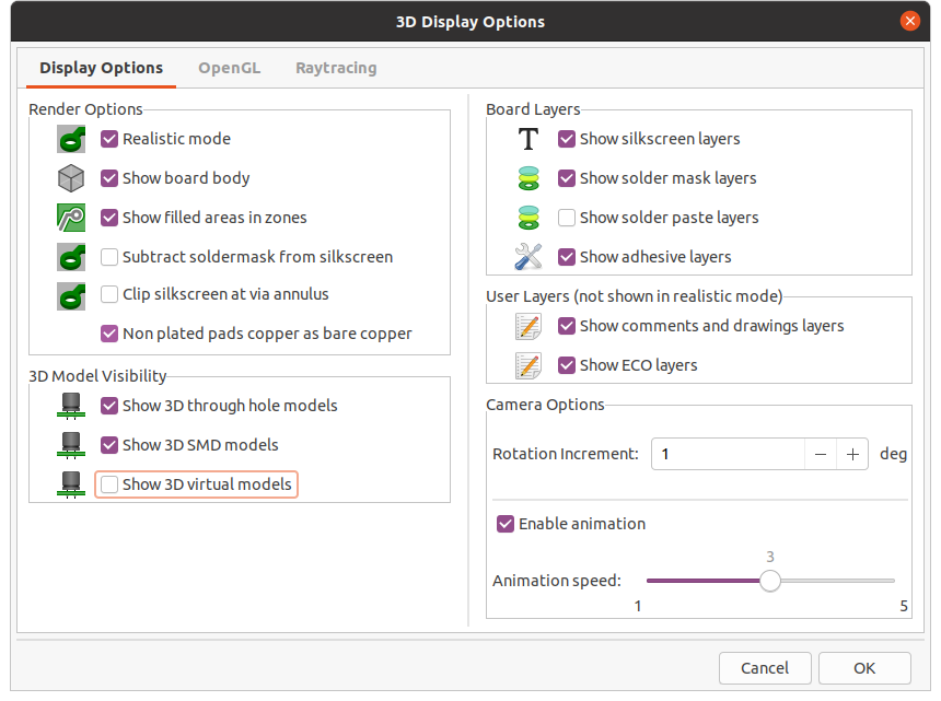
Those of us using KiCad for circuit board design know how useful the built-in 3D viewer and associated (rudimentary) renderer is. KiCad renderer is getting better, but if you want to get there fast, and want to create some amazing photorealistic renders of your PCB, then Blender’s the way to go. Blender can be intimidating to start with, so we’ll walk through a couple of simple steps to go from KiCad VRML export to photorealistic Blender renders.
The KiCad 3D Viewer has seen a few incremental improvements during the course of V6 development:
Plated and Non-Plated Copper
A subtle change has been made in MR#405 by Mario Luzeiro that affects how copper is rendered. The visual difference between plated copper pads and non-plated copper pads will now be visible as well as copper in general.
This image shows a ENIG plated copper hole compared to the surrounding copper traces when the soldermask was turned off.