STM32 and FPGAs In A Tiny Package — Hackaday

Slowly, very slowly, the time when we don’t subject embedded beginners to AVRs and PICs is coming. At a glacial pace, FPGA development platforms are becoming ever more capable and less expensive. [Eric Brombaugh] has been playing around with both ARMs and FPGAs for a while now and decided to combine these two loves into…

via STM32 and FPGAs In A Tiny Package — Hackaday

STM32 and FPGAs In A Tiny Package — Hackaday

STM32-F4 Discovery Breakout Board

[Written by OSH Park engineer Jenner Hanni on Wickerbox Electronics]

stm32-v2-side-L.png

The STM32F4-Discovery development board has columns of male pin headers. I made a breakout board since you can’t plug the dev board into a breadboard, since the two columns on each side will short, and I’ve found the female-to-male jumpers to be unreliable. I made up a breakout board but it’s sadly cost prohibitive at $40 for three boards. Still a quick, fun project.

I’ve open sourced and shared the project at OSH Park.

I started with Jason Lopez’s STM32F4-Discovery Board Eagle schematic and footprint.

For the first test, I placed all the traces on the bottom of the board. Bottom in the layout here is blue. This made it possible to route a breakout board on the PCB router at Portland State’s Lab for Interconnected Devices. I didn’t want to have to plate all the via holes by hand to solder on the bottom and use traces on the top. Been there, done that, not interested. There are 200 vias on this board!

It worked fine, but there’s no silk and I’d really like a better looking board. I uploaded the now-verified Eagle .brd file to OSH Park. Of course, since OSH Park charges $5/square inch for three boards, it was $53.05 for three! Way out of my price budget. Luckily, you can submit designs where two completely separate boards are sitting next to each other on one .brd file.

This is the OSH preview with a cost of $33.95 for three. OSH Park charges for the smallest rectangle that encompasses your design, and you have to leave 100 mils between boards so the fab can mill it out.

It’s still significant, at about $10/board, but I can live with that. The 2×25 and 1×25 female headers also added up. Looks great, though.

The design files are available at the Github repository, and the boards can be ordered for $33.95 for a set of three from OSH Park.

I used these Sullins female headers:

Qty 4 of PPTC251LFBN-RC 1×25 0.1″ for $1.41 each
Qty 2 of SFH11-PBPC-D25-ST-BK 2×25 0.1″ for $2.89 each.

I’d bet you could search on Digikey or Mouser and find a cheaper equivalent.

License

This project is licensed under CERN’s Open Hardware License v1.2.

STM32-F4 Discovery Breakout Board

GPS RF Front-end Board

[Written by OSH Park engineer Jenner Hanni on Wickerbox Electronics]

gpsboard-v2-build.png

Portland State University’s Maseeh College of Engineering and Computer Science runs an innovation program that awards small thousand-dollar grants to students working on interesting projects. In 2011 there were a handful of GPS-related projects that needed a way to work directly with the raw I/Q data coming from the GPS satellites before any processing or correlating had been done.

Background

Commercial off-the-shelf GPS receivers are cheap and ubiquitous but they don’t expose that data. One of my mentors, Andrew Greenberg, developed an open source GPS receiver for his Masters thesis (PDF) in 2005 and suggested I take a look at doing the same thing with current hardware. I said I would if he would help, so together we built a board, built a revision, and are in the process of figuring out what modifications will be needed for a third.

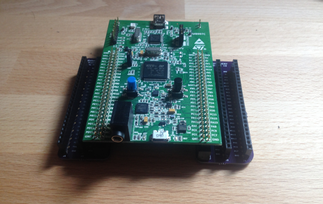
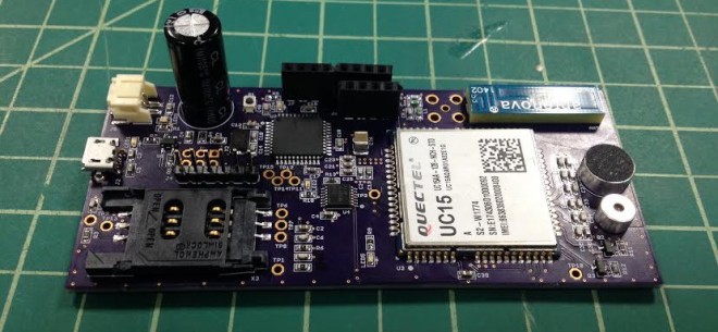
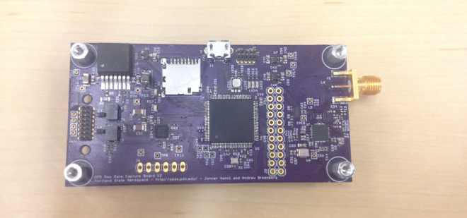
The board isn’t a full GPS receiver. Instead, it’s an “RF front end” board that has a MAX2769 Universal GPS Receiver chip to read the GPS signals and pass them out over something that looks a lot like SPI but isn’t. We chose to place an STM32F407 microcontroller running the ChibiOS embedded operating system on the board to support streaming the data out over Ethernet and USB. We exposed the raw pins over a header between the MAX2769 and STM32F407 to allow a user to skip the microcontroller entirely. We also included an SD card to log the data.

The board does not currently support a battery so it must be powered over USB or Ethernet at all times.

This project is open hardware and software licensed under the 3-clause BSD license and maintained on the Portland State Aerospace Society’s Github account. You can find the bill of materials and Eagle schematics at psas/gps-rf-board and the software as part of psas/stm32.

It’s been a big group effort in the push to get it talking; Andrew, K, Theo, and Kenny at least have helped out with software and modwire soldering, and I might have missed someone.

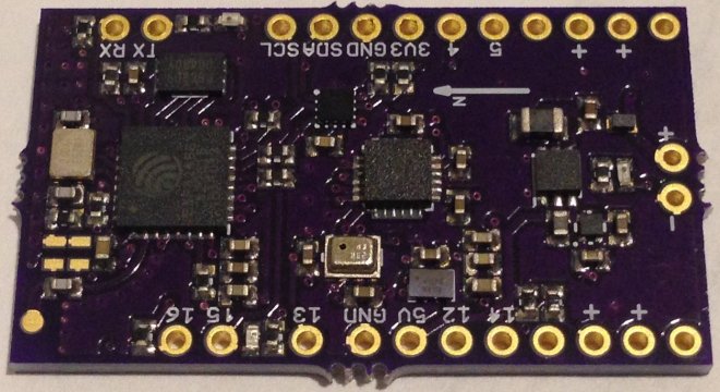
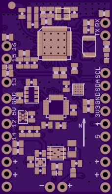
Board Layout Overview

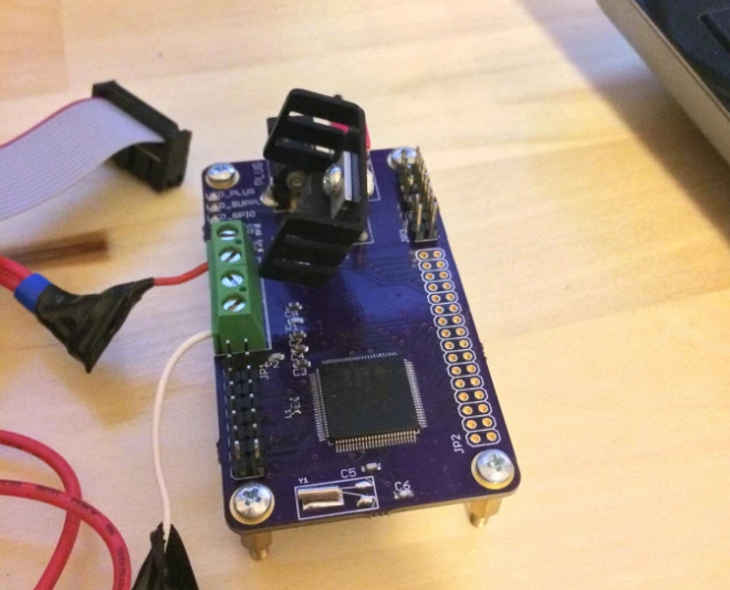
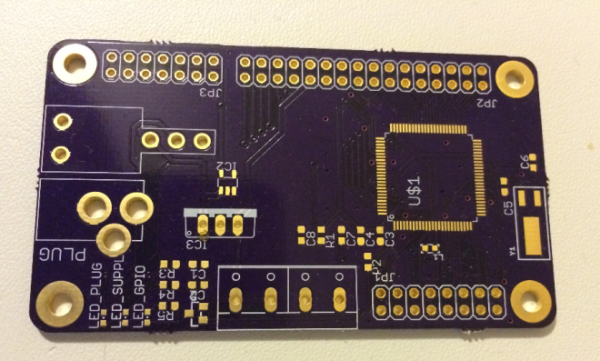
The board has four layers and was ordered from OSH Park.

Power

We can power the board from Rocketnet Ethernet (up to 20V) or over USB (about 5V) so we used an LMZ12001 switching regulator with an input voltage range from 4.5V to 20V to output 3.3V for the digital side of the board. We then used two ultra-low noise MAX8510 LDO linear regulators to provide 2.85V on separate digital and analog supply lines for the RF side of the board.

GPS

The MAX2769 is a tiny 28-pin universal GPS Receiver with a 1.4dB noise figure. The datasheet says we don’t need external SAW filters but we used them anyway. The chip has two LNA inputs and the eval kit is set up for to support both passive and active antennas. We used the MAX2769 Eval Kit as a reference but it was a particularly difficult schematic to work with.

Our board has a single antenna attachment point with a couple of optional circuits that the user chooses by where you populate capacitors and resistors. Option #1 is whether or not to have an LNA1 and its ANTBIAS-pin power circuit. Option #2 is whether to put into LNA1 or LNA2 on the chip.

Output

We use a 100-pin ARM Cortex-M3 STM32F407 running the Portland State Aerospace Society’s version of ChibiOS to program the MAX2769 and to support USB, Ethernet, and an SD card. We also break out raw data signals at pin test points.

Ethernet requires the Portland State Aerospace Society’s Rocketnet connector for programming, data streaming, and power.

A micro-USB connector is available for programming, data streaming, and power.

The micro-SD card is available for data logging.

The serial breakout is two 1×11 0.1” headers which we also used for debug. We ran traces between the two breakouts because we were unsure about some of the pinouts from the MAX2769 and wanted to be sure we could cut traces and easily run modwire.
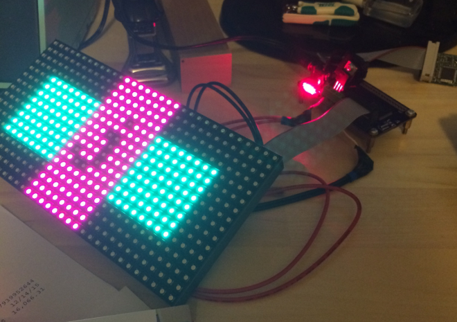
Build

This is the board installed on the avionics module that carries the flight computer, sensor packages, and battery packs. The green board on top is the commercial Crescent GPS unit. The purple board down below is the JennerGPS. They’re both connected to the splitter in the middle, which runs off to the cylindrical patch antenna on the skin of the rocket.

Current Status

The v2 board was flown on the Portland State Aerospace Society’s LV2.3 airframe for Launch 11 on July 20th, 2014, in Brothers, Oregon, to an altitude of 15,000 feet. The hardware was complete but the software on the board was not entirely ready for launch and, anyway, the entire GPS system failed so no data was retrieved.

More information on the launch is available at the PSAS Launch 11 page.

Launch 12 in 2015 carried a third version of the GPS RF front-end board designed and laid out by Andrew Greenberg, and GPS packets were successfully captured.

The Github repository has all the schematics. The current version described here is v2, but the newest version is v3. PSAS welcomes collaboration, but you’ll wan to contact PSAS directly through the main GPS repository. The best way to contribute is to come to a meeting.

It was super helpful to reference Swift Navigation’s Piksi GPS Receiver which uses the MAX2769 chip with an STM32F407 and FPGA.

The first version of this board was funded by the MCECS Innovation Program.

License

This project was released under the BSD “3-clause” license. See here for more information.

GPS RF Front-end Board

RGB LED Panel Controller using MSP432

John Boyd created simple controller for RGB LED panels with the Texas Instruments MSP432 ARM microcontroller:

Screenshot from 2016-07-09 05-26-30

MSP432 RGB LED Panel Controller

I have managed to get it working without issue at 60 FPS [..] I think I could push to above 100 FPS.


Screenshot from 2016-07-09 05-29-00.png

The challenging part of this project was designing the firmware in a way to leverage all of the MSP432 peripherals to reduce the computational requirements for the CPU.

The hardware design files and firmware source code are hosted on GitHub:

 MSP432-RGB-LED-Panel-Controller

Screenshot from 2016-07-09 05-33-53

RGB LED Panel Controller using MSP432

Digital Carburetor Sync Board

[Written by OSH Park engineer Jenner Hanni on Wickerbox Electronics]

IMG_2433

This was a collaboration with Tom Hogue (tz89 from the Venture Rider forum) to translate his prototyped design onto a printed circuit board. He’s done all of the software; my contributions were entirely in hardware.

The Carb Sync Shield monitors the up to six carburetors and displays the vacuum pressure in realtime on an LCD display so the user can make adjustments to the air/fuel mix in each cylinder.

There’s an additional RPM feature that will be useful to set and monitor the idle speed on bikes that don’t have a tachometer.

The kit can be assembled by a novice using a basic soldering iron. The pressure sensors have extra-large surface mount pads and all other components are through-hole.

The shield is compatible with both the Arduino Uno v3 and the Bluetooth-capable RedBear Blend v1. It displays the RPM calculated from each of up to six simultaneous 3.3V or 5V pressure sensors on an LCD display which can be mounted directly or connected with the rainbow jumpers as shown above.

The board draws power from the carrier Uno or Blend board, which in turn can run off a 9V battery or a USB plug. The blue trim potentiometer controls the brightness of the LCD so it’s visible indoors or outdoors. The large switch sets the analog pressure sensor reference voltage to 3.3V or 5V. In the final version of the board, the switch is replaced with a 3-pin header and jumper cap.

Three digital I/O lines are broken out along with dedicated 5V or 3.3V pins to support extra sensors. It’s up to the user to match the sensor voltage on the digital line to the expected operating voltage of the Uno or Blend.

We had the boards fabricated through OSH Park, a local batch PCB service based in Oregon, and did a successful test in early November on Tom’s bike.

Digital Carburetor Sync Board

ESP8266 Flight Controller

2016-03-02T05-15-12.793Z-ESCFC.copter1.jpg.2560x2560_q85.jpg

Kris Winer of Pesky Products designed a brushed motor UAV flight controller using the ESP8266:

ESP8266 Flight Controller

UAV flight controller [..] using the ESP8266EX Tensilica Xtensa system-on-chip, the EM7180+MPU9250+MS5637 (Ultimate Sensor Fusion Solution) for motion sensing and low on-resistance (20 mOhm) n-type DMN2041L MOSFets to drive up to four brushed motors using PWM signals

2016-03-02T03-11-40.889Z-ESCFC.top.08.jpg.2560x2560_q85.jpg

PeskyProducts has shared the board on OSH Park:

ESP8266FlightController.v02b

b5c5510641aee30dbc0a4e303e52a0c1

Order from OSH Park

ESP8266 Flight Controller

3G Cellphone Prototype

[Written by OSH Park engineer Jenner Hanni on Wickerbox Electronics]

finalboard.jpg

David A Mellis designed a DIY 2G Cellphone using the Quectel GSM/GPRS M10 2G module and the Arduino GSM Shield library. I updated David’s design with his permission and replaced the M10 with a Quectel UMTS/HSDPA UC15 3G module.

The modules have different pinouts, slightly different packages, and the UC15 takes 3.3V-4.3V while the M10 took 3.3V-4.6V, which accommodates a 3.7V LiPo battery.

I got the boards back and did an initial build, then handed things over to a local software developer who developed and presented the working cellphone at !!Con:

The Eagle schematic and layout, along with the development notes and bill of materials are available for the first version of the hardware:

Vocabulary

  • GSM – Global System for Mobile Communications, 2G
  • GPRS – General Packet Radio Services, packet data service on 2G and 3G
  • UMTS – Universal Mobile Telecommunications System, 3G
  • HSDPA – High-Speed Downlink Packet Access, allows 3G speeds

Reference

“GSM (Global System for Mobile Communications, originally Groupe Spécial Mobile), is a standard developed by the European Telecommunications Standards Institute (ETSI) to describe protocols for second generation (2G) digital cellular networks used by mobile phones.” -Wikipedia

“General packet radio service (GPRS) is a packet oriented mobile data service on the 2G and 3G cellular communication system’s global system for mobile communications (GSM).” -Wikipedia

“UMTS specifies a complete network system, which includes the radio access network (UMTS Terrestrial Radio Access Network, or UTRAN), the core network (Mobile Application Part, or MAP) and the authentication of users via SIM (subscriber identity module) cards.” -Wikipedia

“High-Speed Downlink Packet Access (HSDPA) is an enhanced 3G (third-generation) mobile-telephony communications protocol in the High-Speed Packet Access (HSPA) family, also dubbed 3.5G, 3G+, or Turbo 3G, which allows networks based on Universal Mobile Telecommunications System (UMTS) to have higher data-transfer speeds and capacity.” -Wikipedia

License

This project is released under the MIT License. Click here for more information.

3G Cellphone Prototype

Monitor plants with Bluetooth LE

Cmoa9VgWcAAScTZ.jpg
JamesCannan created a simple way of monitoring plants with Bluetooth Low Energy (BLE):

Easy Planter

Monitor temperature, humidity, pressure, moisture, light, and has I2C extension pins so that you can add other modules. Information is sent to a phone, and notifies you when it needs something.


The EAGLE schematic and board layout are hosted on GitHub:

github Cannonball2134/EasyPlanter

Monitor plants with Bluetooth LE

STM32F303 + ice5 Development Board

Eric Brombaugh designed this board which pairs ARM Cortex M4 processor with a Lattice FPGA:

f303_ice5

STM32F303 + ice5 Development Board

USB, Micro SD, PMOD and GPIO interfaces allow development of complex projects in control and signal processing.

Schematic Diagram

sch.png

  • STM32F303CCT6 microcontroller:
    • 32-bit ARM Cortex-M4F CPU rated for 72MHz clock
    • 48kB SRAM, 256kB Flash
    • 10 Timers
    • 3x SPI, 2x I2S, 2x I2C, 3x USART
    • 1x CAN, 1x USB Device
    • 37 GPIO pins (20 5V tolerant)
    • 4x 12-bit SAR ADC, 2x 12-bit DACs
    • 7 Analog Comparators, 4 Op-Amps
  • Lattice iCE5LP4K-SG48 FPGA:
    • 3520 LUTs
    • 4 Multiplier/Accumulate blocks
    • 20x 4kb RAMs
    • OTP Non-volatile configuration memory
    • 1 PLL, 2x I2C cores, 2x SPI cores

The microcontroller firmware and FPGA hardware source is hosted on GitHub:

github emeb/f303_ice5


emeb has shared the board on OSH Park:

f303_ice5

124aa008272afeee0ce2d3c70dbaa45f

Order from OSH Park

STM32F303 + ice5 Development Board