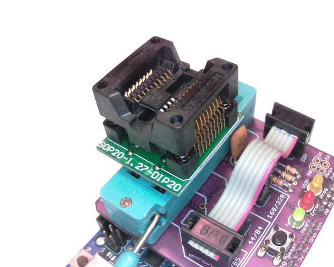
A majority of my projects to date have used DIP package Attiny85, 84, and Atmega328. These are usually programmed beforehand using a ISP shield on an Arduino, or afterwards using the ISP header. My first PCB design, was in fact, a shield which could be used to program the variety of AVR chips I was using. Breadboarding up an Arduino-as-ISP circuit time every time I needed one was error-prone and frustrating.
It occurred to me that since not all projects have ISP headers, there should be some way to program the chips prior to installation. With a little googling, I found SOIC to DIP adapters which can be used to mate up with a DIP ZIF fixture. A SOIC 20 allows me to program the AVR 8-pin, 14-pin, and 20-pin packages!
It used to be hot air soldering gear was exotic, but not anymore. There are plenty of relatively inexpensive choices. Many of these appear to be the same despite having different brand names and model numbers. One that is common and inexpensive is the 858D. These run about $50. [Gabse] has one and decided to…
We think of helping hands as those little alligator clips on a metal stand. They are cheap and fall over, so we tend to buy them and don’t use them. However, if you are willing to put $35 or $40 into it, you can get the newer kind that have–well–tentacles–on a heavy base. [Archie_slap] didn’t…
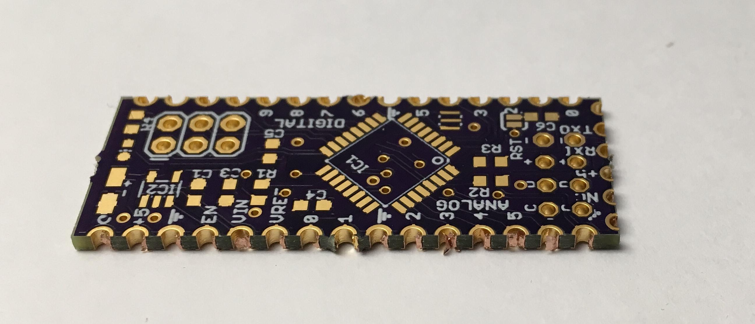
Castellations are small plated edges, typically used for making circuit boards into small PCB modules. These are often seen on wireless modules, such as the ESP8266-12E.
While we don’t offer full support for castellations, they can be fabricated if you don’t mind a few minutes of rework and verification of the PCBs.
Design Considerations
It’s helpful to include a fallback hole near the edge. The ESP8266-12E boards, are a great example here. The extra via allows easy connecting of wires for rework, and makes it easy to salvage a module if the fabricated PCB doesn’t turn out perfectly.
Castellations are simple to call out in most design tools. Simply include a via on the PCB, so the board outline goes through it.
However, due to our panelization process, the castellated vias must be indicated with round pads for copper and stop mask. The pads must also not extend more than 40 mil from the board edge. Square pads or pads that extend far beyond the edge will be trimmed, and the via will not be plated.
It’s also helpful to use a 10 mil wide line for the board outline. With our milling tolerance of 5 mil, this provides a good visual indicator of where the physical board edge might be. The fabricated edge can be anywhere within that line. This is very helpful for fine-pitch castellations with smaller holes.
Callout as seen in a design tool
Rectangular castellations can be made by using vias with round pads as noted above, and adding overlapping rectangular SMD pads. Since these pads are inside the board outline, they will not be trimmed, and will provide additional area for soldering (see below for example).
Cleaning up the final boards
We make a best-effort to minimize support tabs on castellated edges, but it sometimes happens. In these cases, you’ll need to file the tab off of your edge.
Additionally, the via plating may not be fully removed during the milling process. In some cases it’s smashed next to the edge, where it can cause unwanted connectivity between vias. In others, it’s smashed inside the via, where it will prevent good solder flow. A fine point file or hobby knife will help remove excess plating.
An unreworked castellated PCB, with visible plating stubs
Another version, with tabs on castellated edge and modifications for rectangular pads
We are always surprised how much useful hacking gear is in the typical craft store. You just have to think outside the box. Need a hot air gun? Think embossing tool. A soldering iron? Check the stained glass section. Magnification gear? Sewing department. We’ve figured out that people who deal with beads use lots of fine…
Surface mount PCBs (Part 1) If you look at a circuit board today, you’ll see a beautiful array of surface mount chips and components, including very fine 0.5mm or even 0.4mm leaded devices and BGAs. Some of these ‘exotic’ devices can contain really advanced technology such as high speed ARM microprocessors, flash and high capacity […]
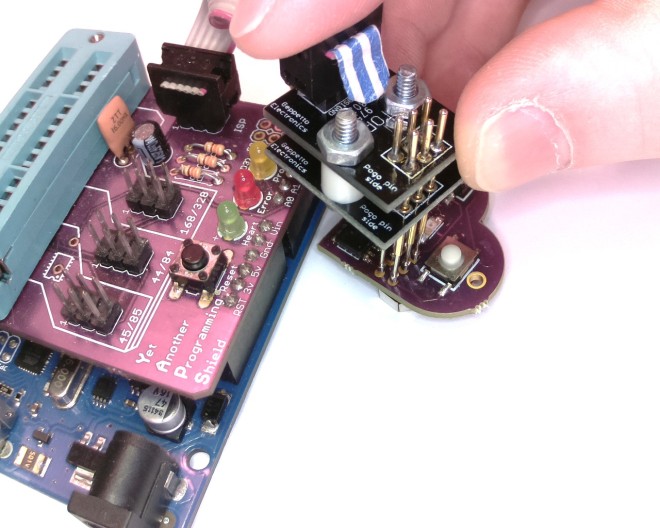
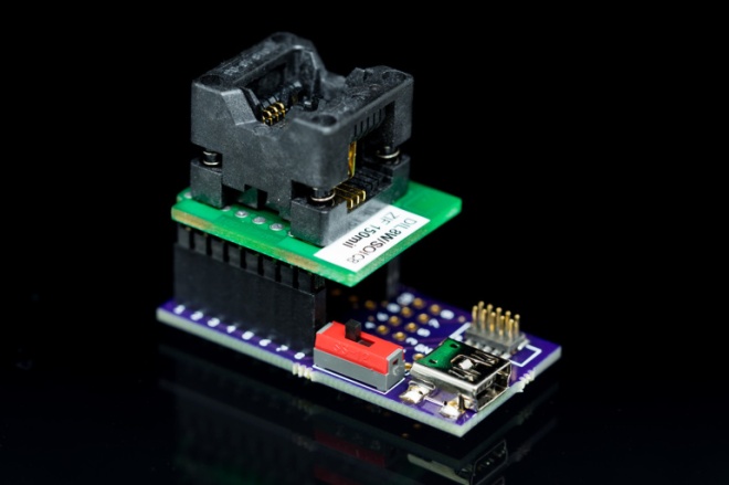
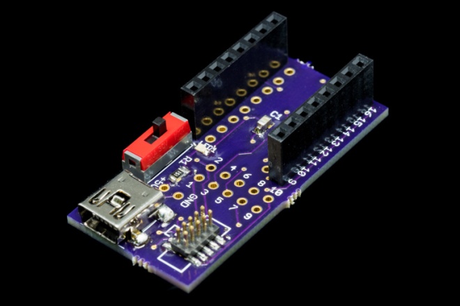
As mentioned in my article about designing a cheap plant watering sensor, I built a small adapter which can be used to pre-program the ATtiny13A. This is necessary, because once soldered on the board, I only have a debugWire interface, which has to be enabled first.
The adapter has a small 50mil JTAG header, where the Atmel ICE can be connected with the board. There is also room for a USB mini jack, which is used to power the MCU while programming. A small on-off switch is used to power the MCU and a LED is placed as indicator to see if the MCU has power.
One of the DIL/ZIF adapters is mounted on top of the female headers. Most of the adapters for SO-8, SO-14 and SO-16 will work with this board.
To make the board more versatile, I added a number of jumpers and solder points. By default, the adapter is connecting to the right pins for the ATtiny13A, but you can cut these routes and solder wires onto the board to implement any kind of connection you like.
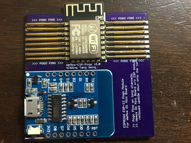
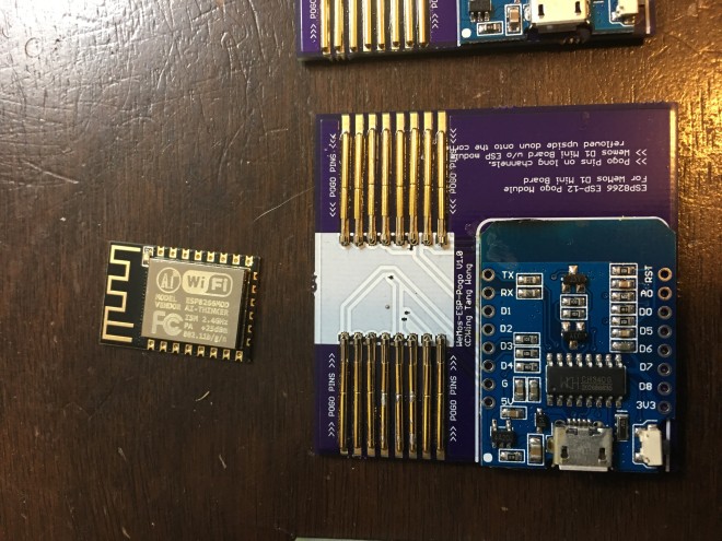
Upcycles D1 Mini Wemos board to create a USB connected ESP8266 Pogo pin jig
This is a board designed to take a WeMos D1 Mini board(with the ESP module removed) and use it as a USB interface with built-in reset/flash functionality for bare ESP8266 modules similar to the ESP-12 units.
I personally love the concept of electronic boards connected in “slots” (vertically attached to a horizontal board), like most industrial-grade PLC’s or even our desktop’s expansion cards (video, sound memory): it saves a lot of space and adds more functions to the system, all at once!