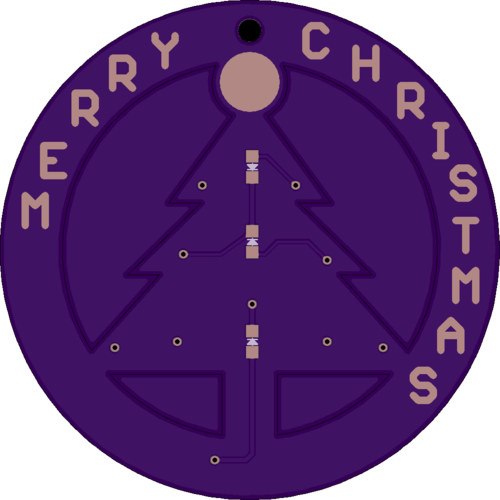
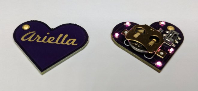
Uri Shaked designed this heart-shaped flashlight PCB for his girlfriend’s birthday:
The design files are available on GitHub:
urish/heart-ariella
Uri Shaked designed this heart-shaped flashlight PCB for his girlfriend’s birthday:
The design files are available on GitHub:
We like the novel orientation of pogo pins that Wing Tang Wong used in this board design:
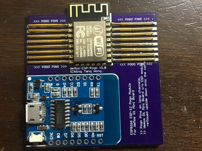
Upcycles D1 Mini Wemos board to create a USB connected ESP8266 Pogo pin jig
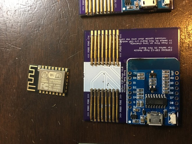
This is a board designed to take a WeMos D1 Mini board(with the ESP module removed) and use it as a USB interface with built-in reset/flash functionality for bare ESP8266 modules similar to the ESP-12 units.
The design files are available on GitHub:
 ESP8266 Programming D1 Mini Pogo Jig V1
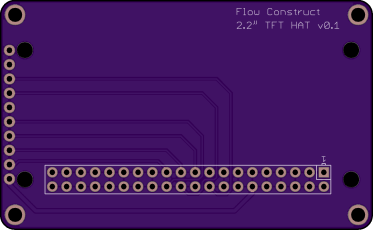
Brian Solon designed this compact board to add an Adafruit 2.2″ TFT LCD display to the Raspberry Pi Zero:
![]()
The design files are available on GitHub:
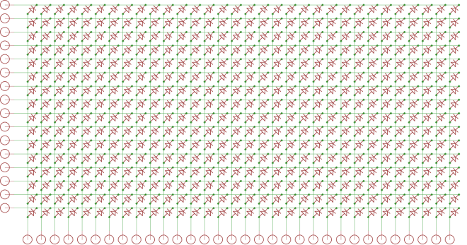
Ted Yapo is designing a display for his LED Oscilloscope Mk. II and decided to automate the process:
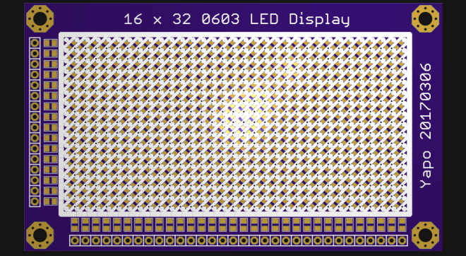
I painstakingly drew the schematic for 512 LEDs in this display, then endured the drudgery of laying out the board. The whole process took about 45 seconds. Yes, I wrote a few Eagle User Language Programs (ULPs) (elapsed time after the scripts were written and debugged). The previous time I wrote one was last century to lay out a circular LED clock face. I figured it was about time I regained those skills.
The EAGLE ULPs are on GitHub:
Eagle scripts for LED matrix display generation
We’re huge fans of Sparkfun’s old school ProtoSnap kits. These include a small support tab with traces running between different sections of the board. They’re great for kit designs, allowing for both immediate out-of-box functionality, and eventual customization.
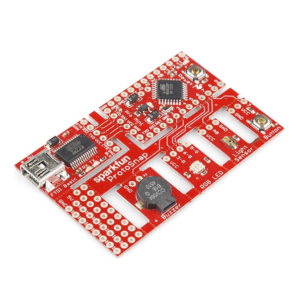
These designs are almost always unique, since the number of shapes, sizes, and orientation varies wildly. The design also may need adjusting based on the intended user.
in orientation, intended usage, and shape. As a result, a bit of experimentation is always going to be required. However, here’s a few design tips to get things going.
Since these typically are for kits, the most likely failure that will occur is a pulled up trace. This is when the trace on the two boards doesn’t break, and starts pulling up traces inside your layout. Not good. Fortunately, the design can account for this in several ways.
Any of these techniques will generate a “stress concentration point” for a pulled up trace. This will cause a the trace to tear in a well-defined place, ensuring that it won’t affect your board.
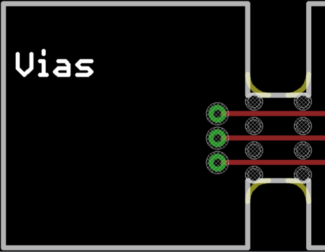
The simplest one simply having vias near the tab, as seen on the sparkfun board above. A ripped up trace will usually break at the edge of the via pad.
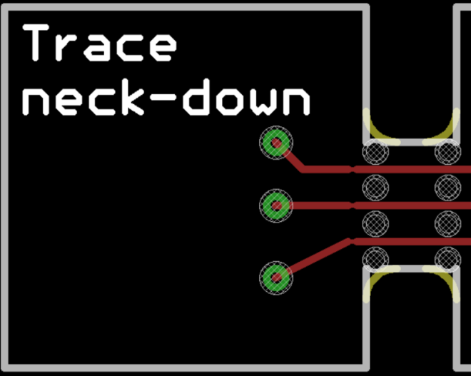
Another option is to actually narrow the trace near the board edge. This takes up less space than a via, but still provides a good weak point in a desirable location. However, make sure you don’t go too far below the design rules!
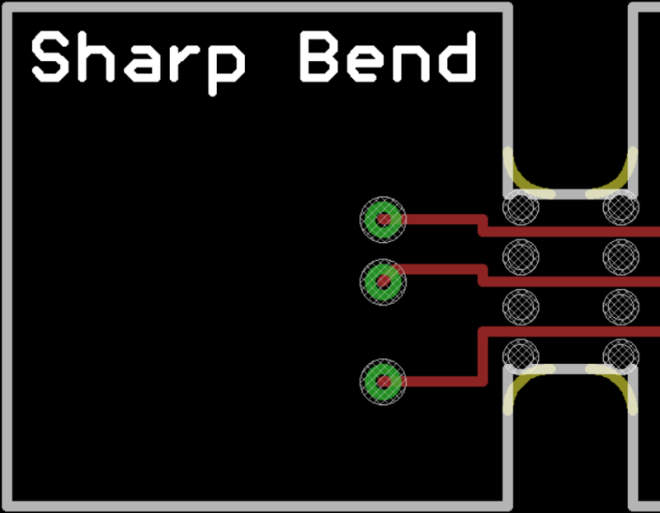
The last option is less ideal, but may suit certain layouts. Simply jog the trace, creating a 90° bend or two.
Here’s the measurements on our typical support tabs. Your design may require different configurations, so these are a rough guideline.
Typical tabs have the following features
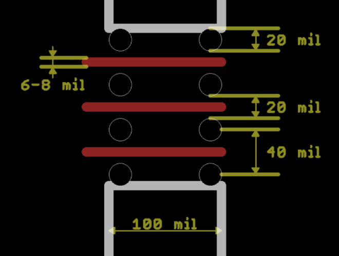
Note, the milling tool will add a 34 mil corner radius on the tabs. As a result, you can place the outermost holes tangent to the tab edge.

Eagle is a household name for all Hackaday regulars. Here’s your chance to learn about upcoming features, get your ‘how do I do this in Eagle?’ questions answered, and get your wishlist items heard. Join us on Friday at 12:00 PST for a live Hack Chat about the Eagle PCB Design software. Hosting this week’s…
via Friday Hack Chat: Eagle PCB Design with Matt Berggren — Hackaday
Star Simpson, creator of Circuit Classics, gave this excellent talk at Hackaday Supercon:
Over the last decade or so, the cost to produce a handful of custom PCBs has dropped through the floor. Now, you don’t have to use software tied to one fab house – all you have to do is drop an Eagle or KiCad file onto an order form and hit ‘submit’.
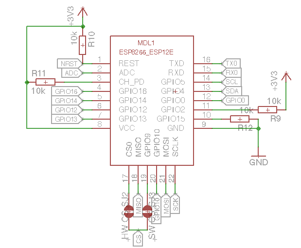
Daniel Grießhaber created this convenient tool to test your WiFi Security against attackers:
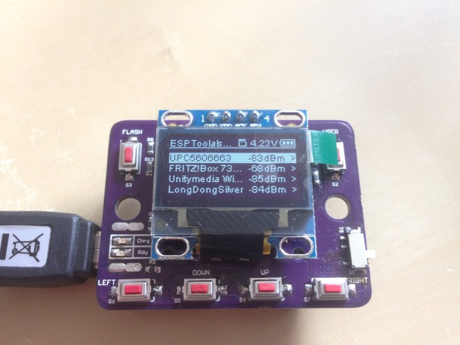
Demonstrate how easy it is to crack a WiFi Password or jam your WiFi so you can’t access the internet. Designed for education and self-tests.
ESPTool has the following hardware:
The design files and source code are available on GitHub:
 dangrie158/ESPTool
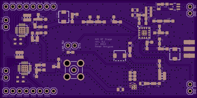
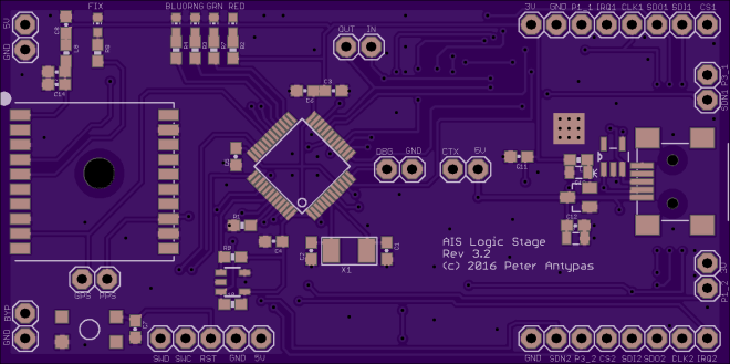
 Open Source AIS Transponder (Class B)
This is the first ever (that I’m aware of) attempt at creating an open source AIS transponder
On the hardware side, the design is based on two Silicon Labs 4463 transceiver ICs and an STM32F302CBT6 ARM Cortex M4 microcontroller. One of the SiLabs ICs acts as a transceiver, while the other IC works as a receiver only. In receiver mode, each IC tunes to a different channel. When a transmission is scheduled, the ICs swap channels if the transceiver is not listening on the next transmit channel. This configuration may be construed as a violation of the AIS specification, but it makes for a much simpler PCB layout and negates the need for a 3-position RF switch.
There are two programs that need to be installed on the flash. The bootloader and the main application.
petera650 has shared the boards on OSH Park:
![]()
![]()