IceZero FPGA Board for Raspberry Pi

Black Mesa Labs created this board that adds a Lattice FPGA to a Raspberry Pi:

ice_zero_with_pi_zero

IceZero FPGA Board for RaspPi

BML has been very much enchanted with the Lattice FPGA boards for Raspberry Pi, IcoBoard , BlackIce and IceHat. The IceZero board is a BML creation that attempts to combine the best features of all 3 boards into a single design.

screenshot-at-2017-02-11-12-23-44

IceZero features common with other designs

  • Fully Open-Source Hardware and Software Design.
  • Lattice ICE40HX4K FPGA that supports Clifford Wolf’s Project IceStorm tool chain.
  • Interfaces to Raspberry Pi 2×20 GPIO Header for both power and bus interfaces.
  • PROM programmable directly from Rasp Pi, no JTAG programmer required.
  • External SRAM, supporting soft CPU core designs ( code execution ).
  • Extra large SPI PROM, supporting soft CPU core designs ( code storage ).
  • Industry standard PMOD expansion headers

sump2_on_ice_zero

IceZero features that are BML specific

  • Mesa Bus Protocol 32 MHz SPI link between CPU and FPGA.
  • 2-Layer PCB design. Orderable via OSH-Park or Gerbers for Downloading.
  • FTDI 1×6 USB Serial Cable header for use with PC instead of Pi ( or as a soft CPU debug Trace Port ).
  • Single Pi UART plumbed to FPGA for muxing to multiple external serial devices.

BlackMesaLabs has shared the board on OSH Park:

bml_ice_zero_19_02.zip

BML IceZero Lattice ICE40 FPGA for RaspPi

db079498cc7f080afc8ce1732dc887d9

Order from OSH Park

IceZero FPGA Board for Raspberry Pi

Learn, Teach and Make with the Tinusaur

Last week we’ve launched our Indiegogo crowdfunding campaign and, as of a few minutes ago, we’ve reached 1/3-rd of our goal already. In case you’re not familiar what the Tinusaur project is about … A small board with a tiny chip on it that comes as an assembly kit – a small package with parts and you […]

via Indiegogo Campaign is Almost Halfway Through — The Tinusaur

Learn, Teach and Make with the Tinusaur

Onion Omega2 Breakout

tumblr_ojbxowFrFv1tja38uo3_1280.jpg

Onion Omega2 Breakout

My Omega2 Onion shield, using a AMS1117 for 3.3V and CH340G for USB to serial. Kind of ugly soldering here as I didn’t have a tip for the syringe to dispense solder paste, so I just smeared it all over and hoped it reflowed well. It kind of did, but I had a solder blob short on pin 14 +15 on the CH340G, so I just lifted those two legs off the board. I was so eager to get this board tested that I forgot to check that I had these 2mm pin headers. I had just enough to get this thing tested. Time to order more 🙂

tumblr_ojbxowfrfv1tja38uo2_1280

Jensa has shared the board on OSH Park:

Onion Omega2 Breakout

fe1620694e5f9a5bb93bbfb970d31ff0
Order from OSH Park

Simple breakout board using the dirt cheap IC’s CH340G ($0.30/each on ebay) for Serial and a AMS1117-3.3 ($0.025/each) for power. Breaks out all pins from 2mm to 2.54mm headers. Plugs nicely into two small breadboards for prototyping.

Onion Omega2 Breakout

Making a USB DAC + Headphone Amp [update]

img_20170202_181622

It’s been a while since I last wrote *ahem* lies *cough* on this project. I am currently a little bit torn whether I should keep writing it here or start posting to my new hackaday.io presence… Anyway here is a brief update: TL;DR I now have a working standalone unit — USB in, headphone out […]

via Making Myself a USB DAC + Headphone Amp — Interim Update — Frog in the Well

Making a USB DAC + Headphone Amp [update]

Protosnap

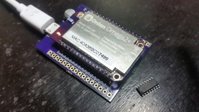
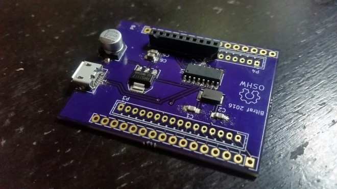
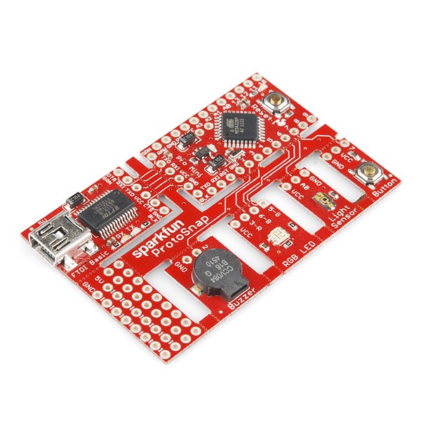
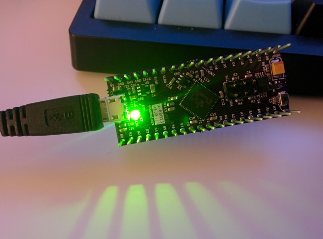
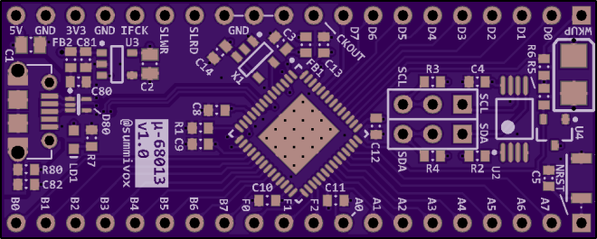
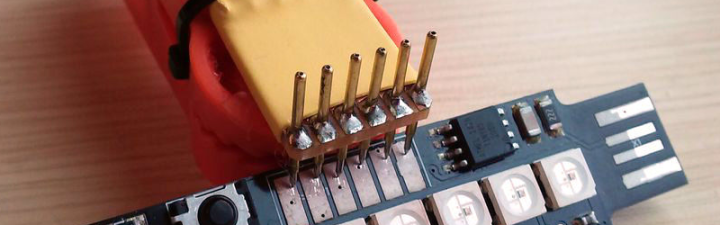
We’re huge fans of Sparkfun’s old school ProtoSnap kits. These include a small support tab with traces running between different sections of the board. They’re great for kit designs, allowing for both immediate out-of-box functionality, and eventual customization.

0lsnm_br3taavxnql
Due to our shipping and panelization process, this type of board is not fully supported, but can be fabricated with careful consideration and experimentation.

Design Considerations

These designs are almost always unique, since the number of shapes, sizes, and orientation varies wildly. The design also may need adjusting based on the intended user.

in orientation, intended usage, and shape. As a result, a bit of experimentation is always going to be required. However, here’s a few design tips to get things going.

  • Always ensure that after snapping, you can connect the boards together easily. A small header pinout near the tab works most of the time, but some designs might work best with a special connector.
  • Tab width is critical. If the tab is too narrow, it will not hold the board together well. Too wide, and it becomes difficult to break apart. 3-5 trace/hole pairs works best.
  • Hole size / pitch. The best tabs have between 20-30 mil of material between the holes. A hole size of 25 mil generates pretty good tabs.
  • Design permitting, having multiple tabs with 2-3 holes is better than one huge tab with 6 or more connections.
  • Adding traces on both top and bottom of a tab is likely to result in difficult snapping. Consider instead using more tabs, or adding instructions to score the traces.
  • Tab and board placement: Remember that your users has to remove these! If the boards are badly positioned, the tabs aren’t “snapped” as much as they are “twisted”. This can result in unusual failures.

Designing for Failures

Since these typically are for kits, the most likely failure that will occur is a pulled up trace. This is when the trace on the two boards doesn’t break, and starts pulling up traces inside your layout. Not good. Fortunately, the design can account for this in several ways.

Any of these techniques will generate a “stress concentration point” for a pulled up trace. This will cause a the trace to tear in a well-defined place, ensuring that it won’t affect your board.

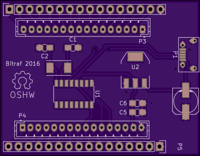
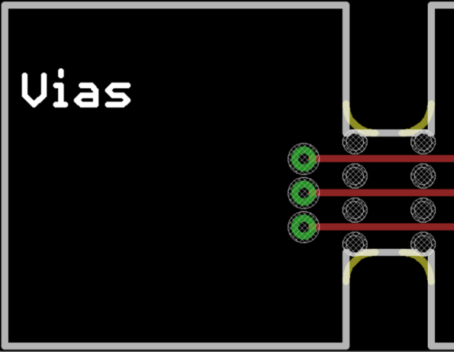
The simplest one simply having vias near the tab, as seen on the sparkfun board above. A ripped up trace will usually break at the edge of the via pad.

0u2dr3nu2dsf7ip8_

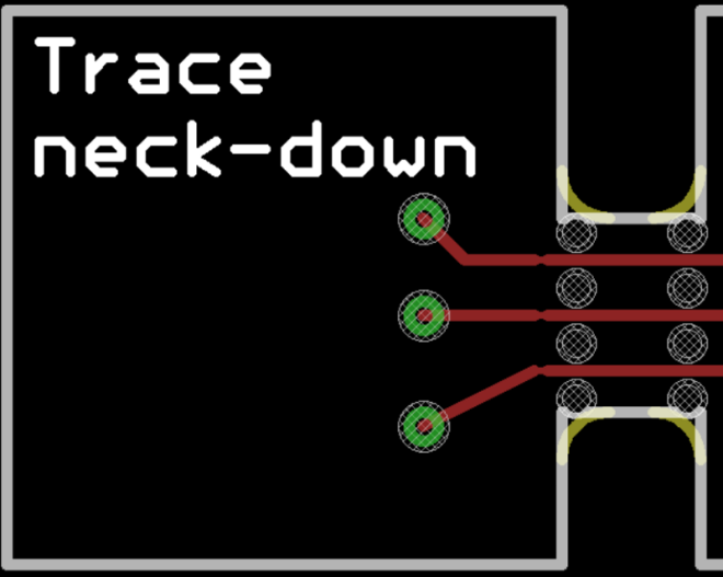
Another option is to actually narrow the trace near the board edge. This takes up less space than a via, but still provides a good weak point in a desirable location. However, make sure you don’t go too far below the design rules!

0-_q8d8anjviisrqn

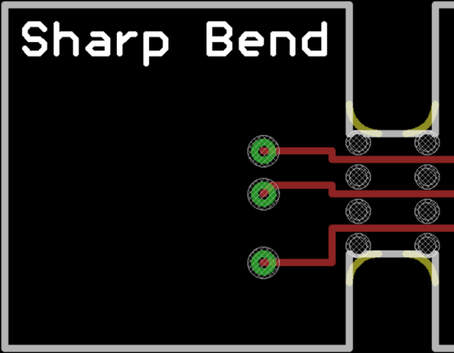
The last option is less ideal, but may suit certain layouts. Simply jog the trace, creating a 90° bend or two.

0pqpeob5lt4fobxon

Indicating on the design

Here’s the measurements on our typical support tabs. Your design may require different configurations, so these are a rough guideline.

Typical tabs have the following features

  • 20-25 mil drill hits
  • 20-25 mil between the edge of the drilled holes
  • roughly a 40 mil drill pitch
  • 2-5 holes per tab (3-4 recommended)
  • Holes tangent to the original board outlines

0cftx3ethihgsbtlg

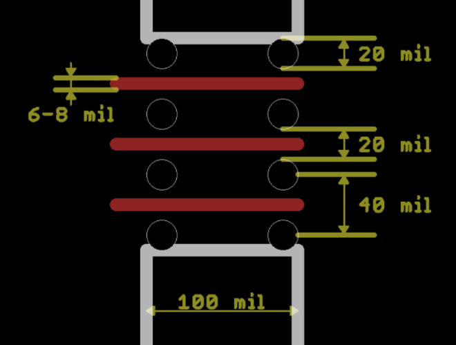
Note, the milling tool will add a 34 mil corner radius on the tabs. As a result, you can place the outermost holes tangent to the tab edge.

Failure modes (and how to cope)

  • Pulled up traces? Need to add a break closer to the edge, or score the board before snapping. Try to handle this on a design revision before a full kit.
Protosnap

Cypress FX2LP High-Speed USB Controller

Yin Zhong designed this dev board for Cypress FX2LP™ microcontroller:

750471485341005936-1

μ-68013: a High Speed USB2.0 MCU breakout

Cypress’s FX2LP (CY7C6801x) is one of the smallest footprint MCUs that offer a high-speed USB (480 Mbit/s) device peripheral with built-in PHY (many others lack the PHY!). It contains a 8051 core for bookkeeping and setting up data streams through its hardware multiplexed parallel FIFO interface to/from an external processor, be it MCU, DSP, or FPGA/CPLD.

This is a breadboard-friendly minimal system PCB for CY7C68013 in QFN56 package. It integrates 3.3 V power supply, core clock, reset circuit/button, and I2C EEPROM (the MCU does not have built-in flash). It breaks out all IO pins through 2 rows x 20 pins 0.1″ pitch headers with 0.7″ row spacing.

summivox has shared the board on OSH Park:

20170112-0057 CY7C68013-v1.0.zip

3ff564ec93a66d415384b740fe7db92f.png Order from OSH Park

Cypress FX2LP High-Speed USB Controller

Analog CPU Gauge

Adam Fabio created this analog gauge to show your computer’s CPU utilization:

Analog CPU Gauge

The goal of this project was to build an analog gauge to display computer CPU utilization. I’ve always been fond of classic analog gauges. Most CPU Gauges are either digital on screen displays, or implemented with an LCD mounted in a drive bay

3404761390189001179

The goal of this project was to build an analog gauge to display computer CPU utilization. I’ve always been fond of classic analog gauges. Most CPU Gauges are either digital on screen displays, or implemented with an LCD mounted in a drive bay.

3060511390157116809

I’d always wanted a CPU gauge for my computer. Ok, and a bandwidth gauge for my router. You name it, I want a nice analog gauge for it. It always seemed a bit silly to use an true galvanometer based analog gauge for signals that are inherently digital.

8130331390188227204

The board is available on Tindie:

tindie-logo2x

Analog Gauge Stepper Breakout Board

Tiny stepper motors for analog gauges and the like!

Analog CPU Gauge

PCB Design Guidelines to Minimize RF Transmissions

screenshot-at-2017-01-27-10-24-11

 writes on Hackaday:

PCB Design Guidelines to Minimize RF Transmissions

There are certain design guidelines for PCBs that don’t make a lot of sense, and practices that seem excessive and unnecessary. Often these are motivated by the black magic that is RF transmission. This is either an unfortunate and unintended consequence of electronic circuits, or a magical and useful feature of them, and a lot of design time goes into reducing or removing these effects or tuning them.

You’re wondering how important this is for your projects and whether you should worry about unintentional radiated emissions [..]

Another good guide is Michael Ossmann’s simple RF design rules:

five_rules.png


PCB Design Guidelines to Minimize RF Transmissions